A kind of preparation method and application of large-area graphene
A graphene and large-area technology, applied in the direction of graphene, nano-carbon, structural parts, etc., can solve the problems of lack of graphene surface functions, unfavorable large-scale production, and restricted material development, etc., to achieve low cost, short cycle, and process The effect of short process
- Summary
- Abstract
- Description
- Claims
- Application Information
AI Technical Summary
Problems solved by technology
Method used
Image
Examples
Embodiment 1
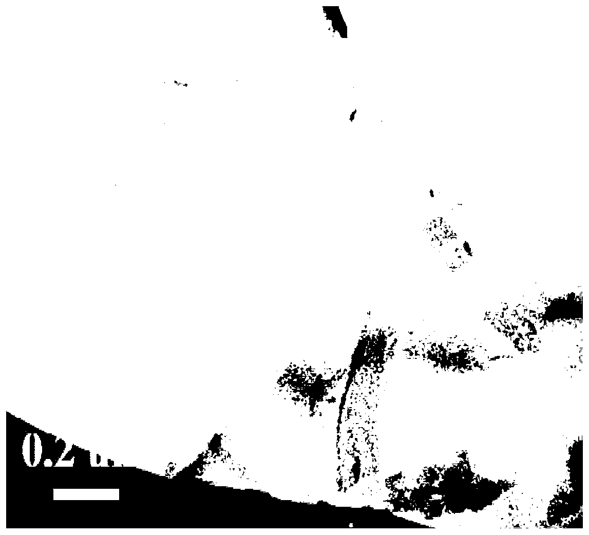
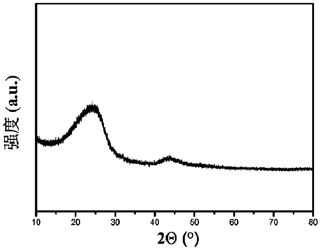
[0039] Mix 0.4g of carbon quantum dots and 4.0g of nickel chloride evenly, and then calcinate them at 700°C for 5h under the protection of Ar gas, with a heating rate of 10°C / min, and naturally cool down. Grind the calcined product into powder, add an appropriate amount of concentrated hydrochloric acid, adjust its pH to neutral, centrifuge at 10000r / min for 10min, wash with deionized water for 5 times, and vacuum dry at 100°C for 12h to obtain a black powder 0.16g. Its scanning electron microscope picture is figure 1 , it can be seen that the product is nano flakes (width can reach 30 μm). figure 2 Its transmission electron microscope picture is consistent with the scanning electron microscope result. image 3 Is its X-ray diffraction spectrum, the product that obtains is graphene carbon.
[0040] Mix the obtained graphene material, sodium carboxymethyl cellulose, and conductive carbon black evenly in a mass ratio of 70:15:15, add an appropriate amount of ultrapure water ...
Embodiment 2
[0042] Mix 0.4g PEG-6000 and 4.0g nickel chloride evenly, and then calcinate it at 750°C for 5h under the protection of Ar gas, with a heating rate of 8°C / min, and naturally cool down. Grind the calcined product into powder, add an appropriate amount of concentrated hydrochloric acid, adjust its pH to neutral, centrifuge at 10000r / min for 10min, wash with deionized water for 5 times, and vacuum dry at 100°C for 12h to obtain a black powder 0.15g. Its scanning electron microscope picture is Figure 4 , it can be seen that the product is a nano-sheet, and the surface area of the graphene material is relatively large (the width can reach 30 μm). Figure 5 Its transmission electron microscope picture is consistent with the scanning electron microscope result.
[0043] Mix the obtained graphene material, sodium carboxymethyl cellulose, and conductive carbon black evenly in a mass ratio of 70:15:15, add an appropriate amount of ultrapure water to make a slurry and apply it on th...
Embodiment 3
[0045] Mix 0.4g carbon quantum dots and 4.0g nickel chloride evenly, and then 2 Under gas protection, it was calcined at 800°C for 4h, the heating rate was 10°C / min, and the temperature was lowered naturally. Grind the calcined product into powder, add an appropriate amount of concentrated hydrochloric acid, adjust its pH to neutral, centrifuge at 10000r / min for 10min, wash with deionized water for 5 times, and vacuum dry at 100°C for 12h to obtain a black powder 0.13g. Its scanning electron microscope picture is Figure 6 , it can be seen that the product is nano flakes (width can reach 30 μm). Figure 7 Its transmission electron microscope picture is consistent with the scanning electron microscope result.
[0046] Mix the obtained graphene material, sodium carboxymethyl cellulose, and conductive carbon black evenly in a mass ratio of 70:15:15, add an appropriate amount of ultrapure water to make a slurry and apply it on the copper foil, and place it in the After drying ...
PUM
| Property | Measurement | Unit |
|---|---|---|
| width | aaaaa | aaaaa |
| tensile strength | aaaaa | aaaaa |
| width | aaaaa | aaaaa |
Abstract
Description
Claims
Application Information
 - R&D
- Intellectual Property
- Life Sciences
- Materials
- Tech Scout
- Unparalleled Data Quality
- Higher Quality Content
- 60% Fewer Hallucinations
Browse by: Latest US Patents, China's latest patents, Technical Efficacy Thesaurus, Application Domain, Technology Topic, Popular Technical Reports.
© 2025 PatSnap. All rights reserved.Legal|Privacy policy|Modern Slavery Act Transparency Statement|Sitemap|About US| Contact US: help@patsnap.com


