Titanium-doped high-quality silicon oxide film and preparation method therefor
A silicon oxide, high-quality technology, used in semiconductor/solid-state device manufacturing, electrical components, circuits, etc., can solve problems such as the electrical performance and stability of silicon-based devices that cannot be effectively met, and achieve the effect of reducing the formation of charges
- Summary
- Abstract
- Description
- Claims
- Application Information
AI Technical Summary
Problems solved by technology
Method used
Image

Examples
Embodiment 1
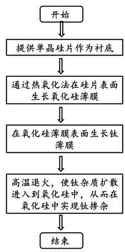
[0024] (1) Select p-type silicon with a crystal orientation of and a resistivity of 10 Ω.cm;
[0025] (2) Use pure oxygen as a protective atmosphere, and use wet oxygen oxidation process to grow SiO on the surface of the silicon wafer described in step (1). 2 Thin film, the thermal oxidation temperature used is 900 °C, and the silicon oxide thickness obtained is 30 nm;
[0026] (3) growing a 10 nm thick titanium film on the silicon oxide surface described in step (2);
[0027] (4) Using argon as a protective atmosphere, subject the silicon wafer described in step (3) to subsequent annealing at 850 °C.
[0028] The subsequent annealing process described in step (4) is aimed at two aspects: on the one hand, through high-temperature annealing under argon gas, the concentration of oxygen vacancies is reduced, and the electrical properties of silicon-based devices and their stability in harsh environments are improved. On the other hand, high-temperature annealing makes titanium...
Embodiment 2
[0030] (1) Select n-type silicon with a crystal orientation of and a resistivity of 50 Ω.cm;
[0031] (2) Use pure oxygen as a protective atmosphere, and use wet oxygen oxidation process to grow SiO on the surface of the silicon wafer described in step (1). 2 Thin film, the thermal oxidation temperature used is 1250 °C, and the obtained silicon oxide thickness is 300 nm;
[0032] (3) growing a 50 nm thick titanium film on the silicon oxide surface described in step (2);
[0033] (4) Using argon as a protective atmosphere, subject the silicon wafer described in step (3) to subsequent annealing at 1150 °C.
Embodiment 3
[0035] (1) Select p-type silicon with a crystal orientation of and a resistivity of 0.1 Ω.cm;
[0036] (2) Use pure oxygen as a protective atmosphere, and use wet oxygen oxidation process to grow SiO on the surface of the silicon wafer described in step (1). 2 Thin film, the thermal oxidation temperature used is 1250 °C, and the obtained silicon oxide thickness is 300 nm;
[0037] (3) growing a 50 nm thick titanium film on the silicon oxide surface described in step (2);
[0038](4) Using argon as a protective atmosphere, subject the silicon wafer described in step (3) to subsequent annealing at 1150 °C.
PUM
| Property | Measurement | Unit |
|---|---|---|
| thickness | aaaaa | aaaaa |
| electrical resistivity | aaaaa | aaaaa |
| thickness | aaaaa | aaaaa |
Abstract
Description
Claims
Application Information
 - R&D
- Intellectual Property
- Life Sciences
- Materials
- Tech Scout
- Unparalleled Data Quality
- Higher Quality Content
- 60% Fewer Hallucinations
Browse by: Latest US Patents, China's latest patents, Technical Efficacy Thesaurus, Application Domain, Technology Topic, Popular Technical Reports.
© 2025 PatSnap. All rights reserved.Legal|Privacy policy|Modern Slavery Act Transparency Statement|Sitemap|About US| Contact US: help@patsnap.com