
Tunable laser based on graphene FP cavity

A technology for tuning lasers and graphene, used in lasers, laser parts, semiconductor lasers, etc., can solve the problems of uncompact device structure, slow tuning speed, difficult integration, etc., to reduce packaging costs, increase range, and improve tuning. effect of speed

Inactive Publication Date: 2017-05-10
UNIV OF ELECTRONICS SCI & TECH OF CHINA
View PDF4 Cites 8 Cited by
  • Summary
  • Abstract
  • Description
  • Claims
  • Application Information

AI Technical Summary

Problems solved by technology

[0006] The present invention solves the problems in the prior art that the output wavelength range of the laser is narrow, the tuning speed is slow, the structure of the device is not compact and it is difficult to integrate

Method used


Image

  • Tunable laser based on graphene FP cavity
  • Tunable laser based on graphene FP cavity

Examples


Embodiment 1

[0036] combined with figure 1 In this embodiment, the material of the tunable laser substrate 1 based on the graphene FP cavity is n-type doped silicon, and the material of the buffer layer 2 is indium phosphide (InP) or gallium arsenide (GaAs) with a thickness of 1-2 μm, The material of the upper optical cladding layer 9 and the lower optical cladding layer 3 is InGaAsP with a thickness of 0.15-0.3 μm, and the material of the upper barrier layer 8 and the lower barrier layer 4 is InP, InGaAsP, InGaAs or GaAs with a thickness of 1-2 μm The material of the active layer 5 is InGaAs quantum well, InGaAs quantum dot or InGaAsP quantum well with a thickness of 0.1-0.2 μm, and the material of the ohmic contact layer 10 is InGaP or GaAs with a thickness of 0.15-0.3 μm.

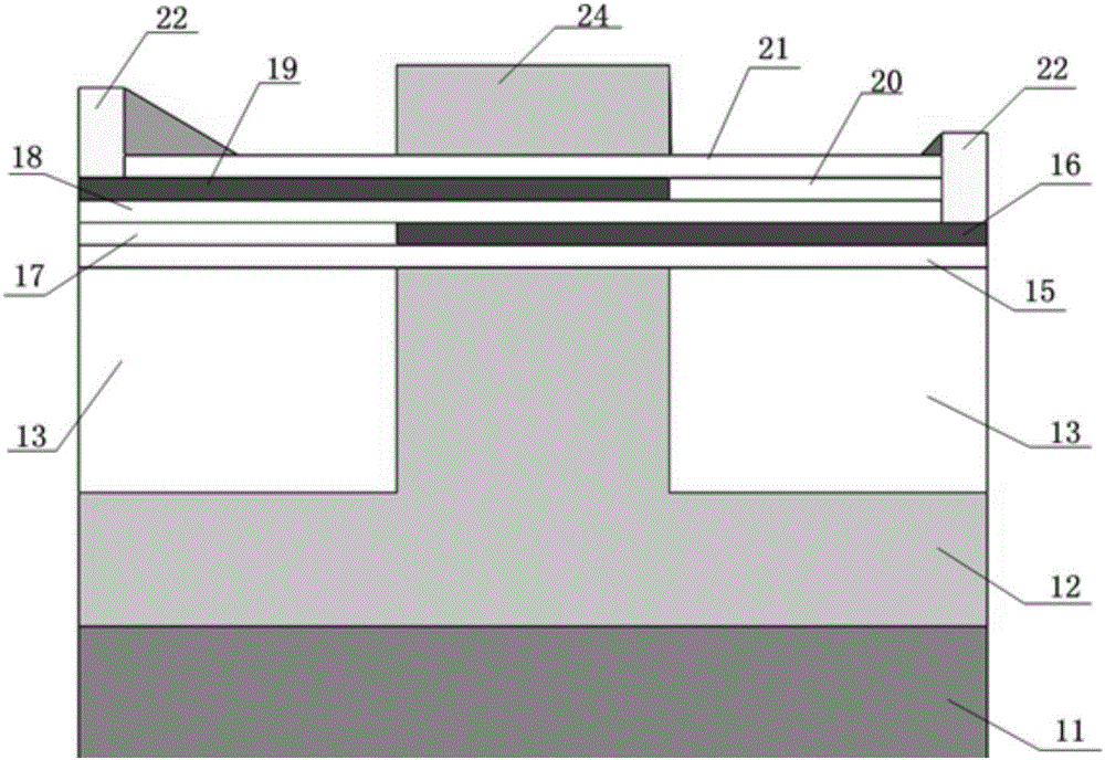
[0037] combined with figure 2 In this embodiment, based on the tunable laser grating structures 6 and 7 of the graphene FP cavity, the material of the substrate 11 is silicon dioxide, and the ridge width of the cor...


PUM


Abstract

The invention discloses a tunable laser based on a graphene FP cavity, which belongs to the technical field of optoelectronic devices and aims at solving the problems that the laser in the prior art is narrow in output wavelength range, the tuning speed is slow, the device structure is not compact and is hard to integrate. The tunable laser based on the graphene FP cavity comprises a substrate (1), a buffer layer (2), a lower optical packet layer (3), a lower barrier layer (4), an active layer (5), an upper barrier layer (8), an upper optical packet layer (9) and an ohmic contact layer (10) sequentially arranged from bottom to top, wherein a first grating (6) and a second grating (7) located at two sides of the active layer (5) are also arranged on the lower barrier layer (4); and the first grating (6) and the second grating (7) are tunable waveguide gratings adopting silicon waveguide-graphene.

Description

technical field [0001] The invention belongs to the technical field of optoelectronic devices, and in particular relates to a tunable laser based on a graphene FP cavity. Background technique [0002] As the size of microelectronic devices is approaching its physical limit, silicon-based optoelectronics, which aims to integrate photonic devices and electronic devices on silicon wafers, has been developed rapidly. Transparent communication band, good mechanical properties, easy processing and other characteristics to make various optoelectronic devices, solve the problems of high cost and difficult integration of various existing devices. Among them, although silicon is an indirect bandgap semiconductor with low luminous efficiency, it is not suitable for direct use as a light source. However, due to the huge application potential of silicon materials, people have not given up on the research on silicon-based lasers. There have been reports of successful use of various lasers...

Claims


Application Information

Patent Timeline
Patent Type & Authority Applications(China)
IPC IPC(8): H01S5/042H01S5/14H01S5/343
CPCH01S5/343H01S5/0427H01S5/141
Inventor 陆荣国刘天良田朝辉杨忠华叶胜威夏瑞杰张尚剑刘永
Owner UNIV OF ELECTRONICS SCI & TECH OF CHINA
Learn More