
Integrated device and fabricating method thereof

a technology of integrated devices and fabrication methods, applied in the direction of piezoelectric/electrostrictive/magnetostrictive devices, transducers, electrical transducers, etc., can solve the problems of reducing the recent trend of size, and achieve the effect of reducing parasitic resistance and increasing tuning rang

Active Publication Date: 2010-04-20
SAMSUNG ELECTRONICS CO LTD
View PDF1 Cites 13 Cited by
  • Summary
  • Abstract
  • Description
  • Claims
  • Application Information

AI Technical Summary

Benefits of technology

The present invention provides an integrated device and its fabricating method that increase tuning range and lower parasitic resistance by integrating an FBAR and a tunable capacitor. The integrated device includes a resonator and a driving electrode layer formed on a substrate, with a first electrode layer and a second electrode layer formed above the substrate and facing the resonator. The first electrode layer is movable towards the resonator by a potential difference generated between the second electrode layer and the driving electrode layer. The integrated device also includes an upper substrate that shifts the first electrode layer towards the resonator when a potential difference over a certain magnitude is generated between the second electrode layer and the driving electrode layer. The fabricating method includes forming a resonator and a driving electrode layer on a first substrate, and forming a first electrode layer and a second electrode layer on a second substrate, connecting the two substrates such that the first electrode layer faces the resonator and the second electrode layer faces the driving electrode layer. The technical effects include increased tuning range and lower parasitic resistance.

Problems solved by technology

However, the filter bank hinders the recent trend toward size reduction.

Method used


Image

  • Integrated device and fabricating method thereof
  • Integrated device and fabricating method thereof
  • Integrated device and fabricating method thereof

Examples


Embodiment Construction

[0038]Certain exemplary embodiments of the present invention will now be described in greater detail with reference to the accompanying drawings.

[0039]The matters defined in the following description, such as a detailed construction and element descriptions, are provided as examples to assist in a comprehensive understanding of the invention. Also, descriptions of well-known functions or constructions are omitted for clarity and conciseness.

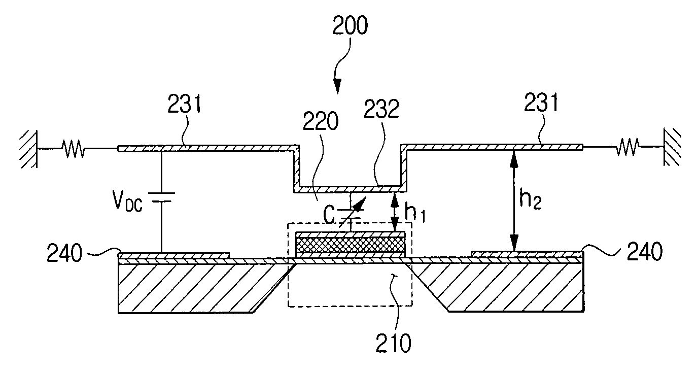
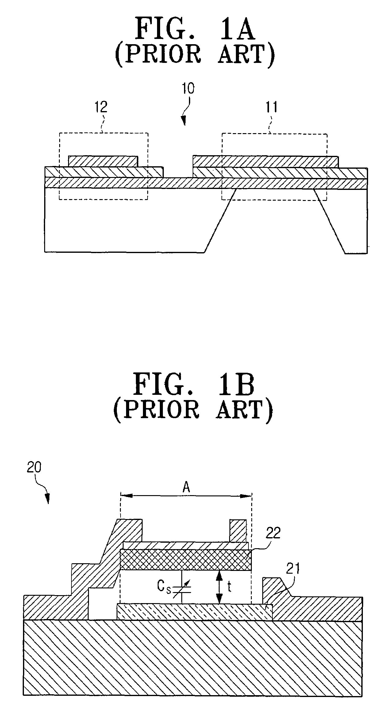
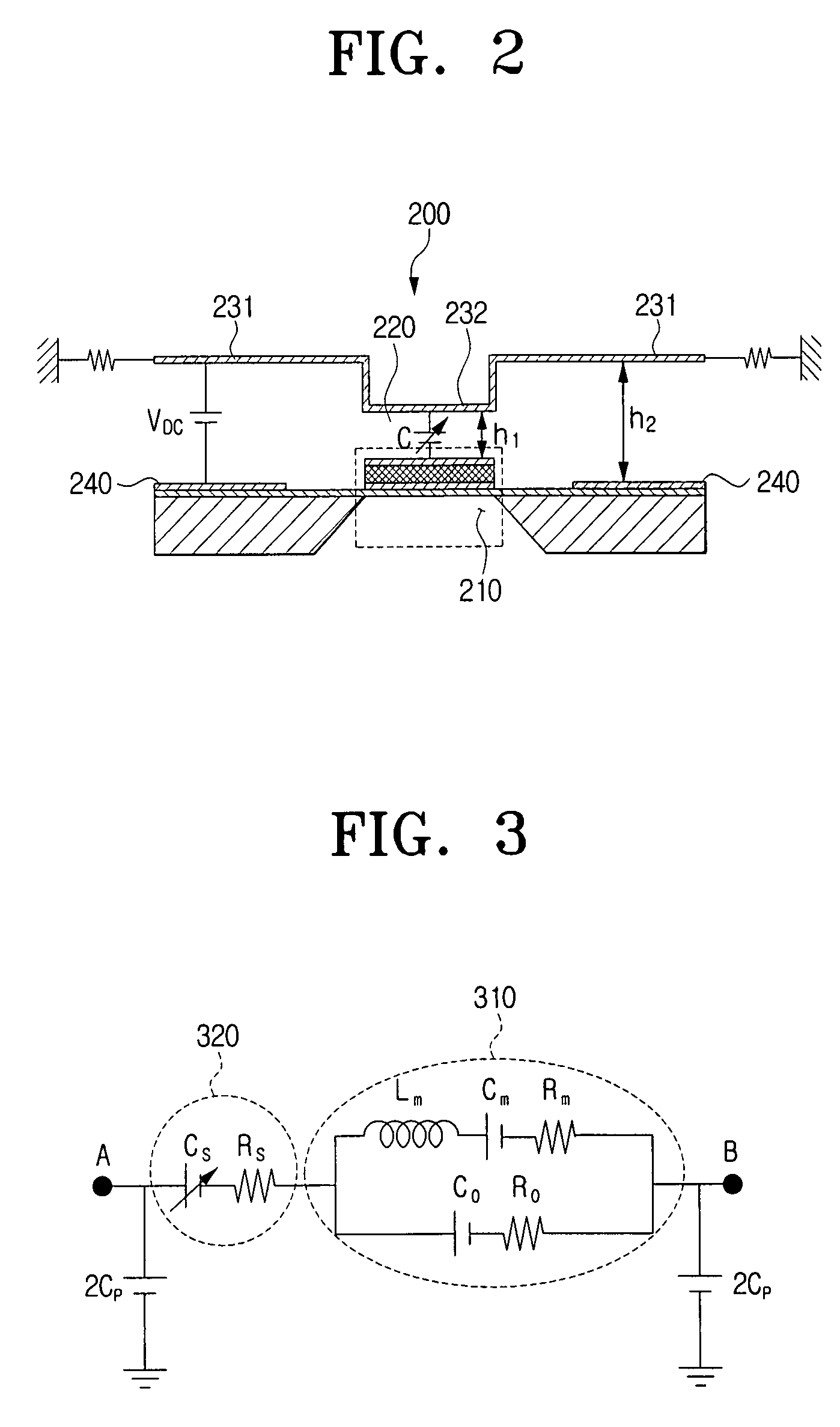
[0040]FIG. 2 is a conceptual diagram of an integrated device according to an embodiment of the present invention. Referring to FIG. 2, the integrated device 200 includes a resonator 210 and a tunable capacitor 220 which are integrated together. The tunable capacitor 220 is formed between the resonator 210 and a first electrode 232 which is disposed above the resonator 210. In more detail, as a potential difference V is generated between a driving electrode 240 and a second electrode 231 which is disposed above the driving electrode 240, the first...


PUM

PropertyMeasurementUnit
thicknessaaaaaaaaaa
areaaaaaaaaaaa
distanceaaaaaaaaaa

Abstract

An integrated device is constructed by integrating an FBAR and a tunable capacitor. The integrated device includes a substrate; a resonator formed on the substrate; a driving electrode layer formed on the substrate apart from the resonator; a first electrode layer formed upwardly apart from the substrate and facing the resonator; and a second electrode layer formed upwardly apart from the substrate and facing the driving electrode layer, the second electrode layer stepped from the first electrode layer. Accordingly, the integrated device can increase the tuning range and mitigate the parasitic resistance.

Description

CROSS-REFERENCE TO RELATED APPLICATIONS[0001]This application claims benefit under 35 U.S.C. §119(a) of Korean Patent Application No. 2006-113303, filed on Nov. 16, 2006, in the Korean Intellectual Property Office, the entire disclosure of which is hereby incorporated by reference.BACKGROUND OF THE INVENTION[0002]1. Field of the Invention[0003]The present invention relates to an integrated device and fabricating method thereof. More particularly, the present invention relates to an integrated device and its fabricating method for increasing a tuning range using a film bulk acoustic resonator (FBAR) and a tunable capacitor integrated together and reducing a parasitic resistance occurring from a discrete connection.[0004]2. Description of the Related Art[0005]Recently, as mobile communication devices, such as cellular phones, are prevalently used, effort has been made to enhance the performance of mobile communication devices and fabricate them to have smaller size and lighter weight....

Claims


Application Information

Patent Timeline
Patent Type & Authority Patents(United States)
IPC IPC(8): H03H9/00H10N30/01
CPCH03H3/04H03H9/174H03H9/0547Y10T29/42H03H3/00H03H9/15
Inventor PARK, EUN-SEOKNAM, KUANG-WOOSONG, IN-SANGKIM, CHUL-SOOPARK, YUN-KWON
Owner SAMSUNG ELECTRONICS CO LTD
Learn More