A kind of rear passivation crystalline silicon solar cell and preparation method thereof
A crystalline silicon solar cell and back passivation technology, applied in the field of photovoltaic solar energy, can solve the problems of difficult process, expensive laser processing equipment, reduced filling factor and photoelectric conversion efficiency, etc., so as to avoid difficult process and improve photoelectric conversion efficiency. , the effect of reducing light loss and carrier recombination loss
- Summary
- Abstract
- Description
- Claims
- Application Information
AI Technical Summary
Problems solved by technology
Method used
Image

Examples
preparation example Construction
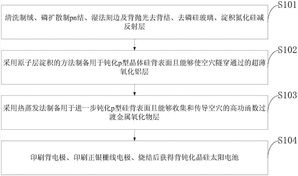
[0031] Such as figure 2 As shown, the preparation method of the back passivated crystalline silicon solar cell provided by the embodiment of the present invention includes:
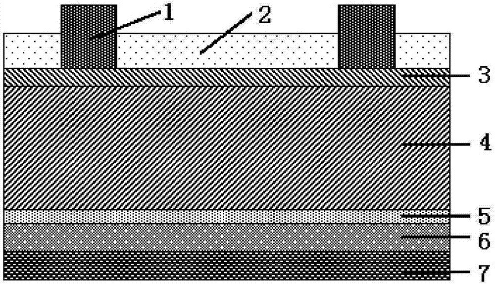
[0032] S101: cleaning texture, phosphorus diffusion to make pn junction, wet edge cutting and back polishing to remove back junction, phosphorus silicon glass removal, deposition of silicon nitride anti-reflection layer;
[0033] S102: using an atomic layer deposition method to prepare an ultra-thin aluminum oxide layer for passivating the back surface of p-type crystalline silicon and allowing holes to tunnel through;
[0034] S103: Preparing a high work function transition metal oxide layer for further passivating the p-type silicon back surface and capable of collecting and conducting holes by using a thermal evaporation method.
[0035] S104: Printing the back electrode, printing the front silver grid electrode, and sintering to obtain a rear passivated crystalline silicon solar cell.
[0036] Furt...
Embodiment 1
[0043] Take 156*156mm 2 The p-type single crystal silicon wafer with a large area is used as the initial material, which is cleaned and textured, pn junction made by phosphorus diffusion, wet edge cutting and back polishing to remove the back junction, phosphorus silicon glass is removed, silicon nitride anti-reflection layer is deposited, and silicon nitride anti-reflection layer is deposited. The rear passivation monocrystalline silicon solar cell is obtained by depositing ultra-thin aluminum oxide layer, depositing non-stoichiometric molybdenum oxide layer, printing back silver electrode, printing front silver grid line electrode, and sintering process. The ultra-thin aluminum oxide layer is prepared by atomic layer deposition method, in which (CH 3 ) 3 Al is aluminum source, high-purity H 2 O is an oxygen source, and reacts at a substrate temperature of 150 degrees Celsius to form a 1nm-thick aluminum oxide layer. The non-stoichiometric molybdenum oxide layer is produce...
Embodiment 2
[0045] Take 156*156mm 2 The p-type polysilicon wafer with a large area is used as the initial material, which is cleaned and textured, pn junction made by phosphorus diffusion, wet edge and back polished to remove the back junction, phosphorus silicon glass is removed, silicon nitride anti-reflection layer is deposited, and super Thin aluminum oxide layer, deposit non-stoichiometric molybdenum oxide layer, print back silver electrode, print front silver grid line electrode, and sintering process to obtain back passivation polycrystalline silicon solar cell. The ultra-thin aluminum oxide layer is prepared by atomic layer deposition method, in which (CH 3 ) 3 Al is aluminum source, high-purity H 2 O is an oxygen source, and reacts at a substrate temperature of 150 degrees Celsius to form a 1nm-thick aluminum oxide layer. The non-stoichiometric molybdenum oxide layer is produced by thermal evaporation. In the process, molybdenum oxide powder with a purity greater than 99.9% is...
PUM
| Property | Measurement | Unit |
|---|---|---|
| thickness | aaaaa | aaaaa |
| thickness | aaaaa | aaaaa |
Abstract
Description
Claims
Application Information
 - R&D
- Intellectual Property
- Life Sciences
- Materials
- Tech Scout
- Unparalleled Data Quality
- Higher Quality Content
- 60% Fewer Hallucinations
Browse by: Latest US Patents, China's latest patents, Technical Efficacy Thesaurus, Application Domain, Technology Topic, Popular Technical Reports.
© 2025 PatSnap. All rights reserved.Legal|Privacy policy|Modern Slavery Act Transparency Statement|Sitemap|About US| Contact US: help@patsnap.com