Method for forming a lightly doped region and method for manufacturing a semiconductor device

A lightly doped region and semiconductor technology, which is applied in semiconductor/solid-state device manufacturing, semiconductor devices, electrical components, etc., can solve the problem of NMOS structure leakage current difficult to suppress activation temperature, reduce manufacturing steps and costs, and suppress leakage current Effect

Active Publication Date: 2019-08-02
WUHAN CHINA STAR OPTOELECTRONICS TECH CO LTD
View PDF4 Cites 0 Cited by
  • Summary
  • Abstract
  • Description
  • Claims
  • Application Information

AI Technical Summary

Problems solved by technology

[0004] The technical problem mainly solved by the present invention is to provide a method for forming a lightly doped region and a method for manufacturing a semiconductor device, which can solve the problems in the prior art that the leakage current of the NMOS structure is difficult to suppress and the activation temperature is high

Method used


Image

  • Method for forming a lightly doped region and method for manufacturing a semiconductor device
  • Method for forming a lightly doped region and method for manufacturing a semiconductor device
  • Method for forming a lightly doped region and method for manufacturing a semiconductor device

Examples


Embodiment Construction

[0021] The following will clearly and completely describe the technical solutions in the embodiments of the present invention with reference to the accompanying drawings in the embodiments of the present invention. Obviously, the described embodiments are only some, not all, embodiments of the present invention. Based on the embodiments of the present invention, all other embodiments obtained by persons of ordinary skill in the art without making creative efforts belong to the protection scope of the present invention.

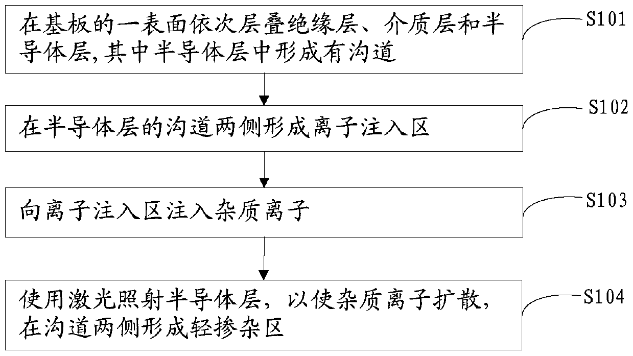
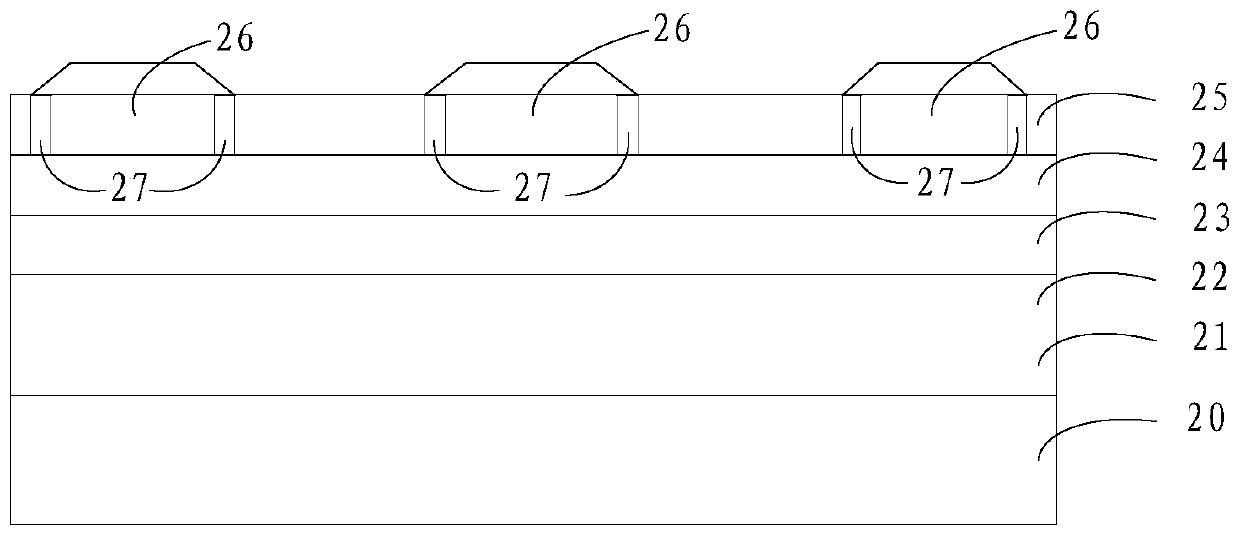
[0022] see figure 1 , figure 1 It is a flowchart diagram of an embodiment of the lightly doped region forming method of the present invention. Such as figure 1 As shown, the lightly doped region forming method of the present invention includes:

[0023] Step S101: sequentially laminating an insulating layer, a dielectric layer and a semiconductor layer on one surface of the substrate;

[0024] Wherein, a channel is formed in the semiconductor layer, and th...


PUM


Abstract

The invention discloses a lightly-doped region formation method and a semiconductor device fabrication method. The lightly-doped region formation method comprises the steps of sequentially laminating an insulation layer, a dielectric layer and a semiconductor layer on a surface of a substrate, wherein a channel is formed in the semiconductor layer; forming ion injection regions at two sides of the channel in the semiconductor layer; injecting impurity ions to the ion injection regions; and irradiating the semiconductor layer by using laser so that the impurity ions are diffused and lightly-doped regions are formed at two sides of the channel. Through the abovementioned mode, the problem that leakage current of an NMOS (N-channel Metal Oxide Semiconductor) structure is difficult to suppress and the activation temperature is relatively high can be solved.

Description

technical field [0001] The invention relates to the technical field of semiconductor manufacturing, in particular to a method for forming a lightly doped region and a method for manufacturing a semiconductor device. Background technique [0002] Flexible display devices have the advantages of lightness, thinness, flexibility, impact resistance, ultra-high waterproof performance, etc., and have a very wide range of applications in the field of wearable devices and some special function displays. [0003] At present, in the technology of preparing flexible devices, the main method is to assemble a flexible substrate on a carrier such as a rigid glass substrate, then prepare a display element on the flexible substrate, and finally separate the flexible substrate from the carrier to obtain a flexible device. In the manufacturing process of flexible devices, the temperature is generally required to be below 450°C, and the current mainstream flexible display devices are manufactur...

Claims


Application Information

Patent Timeline
Patent Type & Authority Patents(China)
IPC IPC(8): H01L29/78H01L21/268H01L21/336
CPCH01L21/268H01L29/66492H01L29/7833
Inventor 方宏
Owner WUHAN CHINA STAR OPTOELECTRONICS TECH CO LTD
Why Eureka
Try Eureka