P-type doping method of oxide semiconductor

A technology of oxide semiconductors and semiconductors, which is applied in the manufacture of semiconductors/solid-state devices, electrical components, circuits, etc., can solve problems such as doping, achieve uniform doping distribution, prevent sublimation, and increase the activation rate.

Pending Publication Date: 2022-04-05
ZHEJIANG UNIV HANGZHOU GLOBAL SCI & TECH INNOVATION CENT
View PDF0 Cites 0 Cited by
  • Summary
  • Abstract
  • Description
  • Claims
  • Application Information

AI Technical Summary

Problems solved by technology

[0004] Aiming at the deficiencies in the prior art, the present invention provides a P-type doping method for oxide semiconductors, which has the advantage of improving the activation rate of acceptor impurities and can quickly solve the existing doping problems

Method used


Image

  • P-type doping method of oxide semiconductor
  • P-type doping method of oxide semiconductor
  • P-type doping method of oxide semiconductor

Examples


Embodiment Construction

[0023] The present invention will be further described in detail below in conjunction with the examples, the following examples are explanations of the present invention and the present invention is not limited to the following examples.

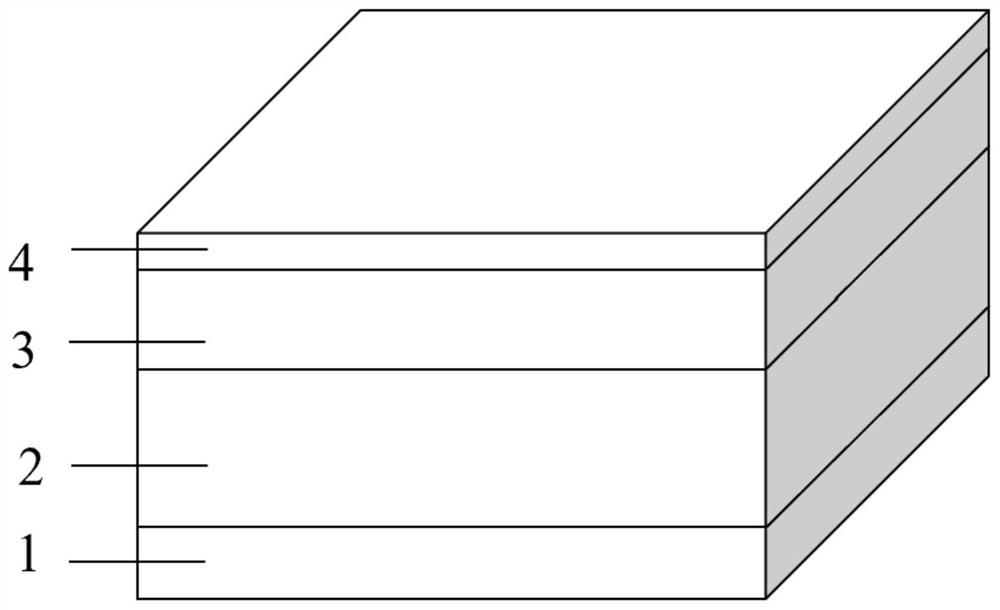
[0024] Such as figure 1 As shown, a P-doped structure includes a substrate layer 1, an epitaxial layer 2, an injection layer 3 and an annealing protection layer 4. The substrate layer 1 and the epitaxial layer 2 can be replaced with different oxide semiconductor substrates and grown epitaxially. The implanted layer 3 is implanted with N element, and its implant dose should be two orders of magnitude or more of the doping concentration of the epitaxial layer. In one embodiment of the present invention, the concentration of the epitaxial layer for the used substrate is 1×10 16 cm -3 , the concentration of the injected N element should be at least two orders of magnitude greater, namely 1×10 18 cm -3 above. And its depth can also be changed...


PUM

PropertyMeasurementUnit
melting pointaaaaaaaaaa

Abstract

The invention relates to a P-type doping method of an oxide semiconductor in the technical field of semiconductors, which comprises the steps of ion implantation, high-temperature annealing and annealing mask protection, the ion implantation is to inject an N element into an epitaxial layer growing on a semiconductor substrate, and the N element is an impurity for providing a hole and forming acceptor doping; according to high-temperature annealing, the injected wafer is placed in a high-temperature annealing furnace to be annealed at the temperature of 1,300 DEG C or above, compared with a traditional post-annealing process, higher temperature is adopted to repair lattice damage generated by injection, the activation rate of an injected doping acceptor is increased, and effective doping is formed. According to the annealing mask protection layer, a layer of AlN thin film is formed on the injected surface, so that diffusion of N during high-temperature annealing is prevented, and sublimation of a substrate material at a high temperature can be effectively prevented.

Description

technical field [0001] The invention relates to the technical field of semiconductors, in particular to a P-type doping method for oxide semiconductors. Background technique [0002] In recent years, more and more attention has been paid to energy saving and emission reduction in the world, which puts forward higher requirements for loss control and efficiency improvement of large power electronic equipment. As an important part of power electronic equipment, semiconductor power devices have received extensive attention from the industry. [0003] Breakdown voltage is an important indicator of semiconductor power devices, indicating the maximum voltage that the device can withstand. Power devices have evolved from silicon material devices to the current third-generation semiconductor material SiC. Because of its large forbidden band width, it is especially suitable for power devices. Now, for SiC, its structure development for withstand voltage has reached a bottleneck, so ...

Claims


Application Information

Patent Timeline
Patent Type & Authority Applications(China)
IPC IPC(8): H01L21/425H01L21/477H01L21/471
Inventor 盛况宛江彬王珩宇任娜
Owner ZHEJIANG UNIV HANGZHOU GLOBAL SCI & TECH INNOVATION CENT
Why Eureka
Try Eureka