InP substrate MOSCAP structure and manufacturing method thereof

A technology of substrate and film, applied in semiconductor/solid-state device manufacturing, semiconductor devices, electrical components, etc., can solve the problems of large leakage and high interface state density, reduce gate leakage, improve reliability, and reduce EOT Effect

Inactive Publication Date: 2017-01-04
INST OF MICROELECTRONICS CHINESE ACAD OF SCI
View PDF7 Cites 0 Cited by
  • Summary
  • Abstract
  • Description
  • Claims
  • Application Information

AI Technical Summary

Problems solved by technology

[0005] The present invention proposes a structure and preparation method of an InP substrate MOSCAP, the main purpose of which is to solve the problem of high interface state density caused by directly growing a high-K gate dielectric material on the InP surface, and at the same time, leakage under the condition of reduced EOT Excessively large, and defects in the reliability of the gate dielectric

Method used


Image

  • InP substrate MOSCAP structure and manufacturing method thereof
  • InP substrate MOSCAP structure and manufacturing method thereof

Examples


Embodiment Construction

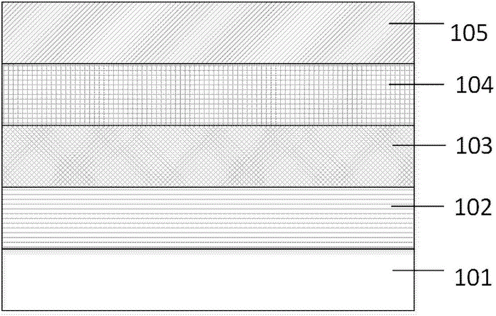
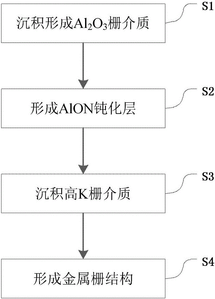
[0026] The present invention proposes a structure of InP substrate MOSCAP and its preparation method. An AlON passivation layer is formed by N2 plasma treatment on the surface of the Al2O3 gate dielectric, and a high-K gate dielectric is grown on the AlON passivation layer, which can effectively repair the Al 2 o 3 Defects in the gate dielectric improve the quality of the gate dielectric, reduce gate leakage, and improve device reliability. The AlON passivation layer improves the Al 2 o 3 The K value and depositing a high-K gate dielectric on the AlON passivation layer reduces the EOT, thereby greatly improving the electrical performance of the InP MOSCAP capacitor. But the passivation layer is not limited to N2 plasma treatment, it can also be grown after Al 2 o 3 Afterwards, N2 annealing is carried out.

[0027] In order to make the object, technical solution and advantages of the present invention clearer, the present invention will be further described in detail below...


PUM


Abstract

The invention discloses an InP substrate MOSCAP structure and a manufacturing method thereof. The method includes the steps that S1, an Al2O3 gate dielectric (102) is deposited on an InP substrate; S2, N2 plasma treatment is conducted on the surface of the Al2O3 gate dielectric to form an AlON passivation layer (103); S3, a high-K gate dielectric (104) is deposited on the AlON passivation layer; S4, a metal gate structure (105) is formed on the high-K gate dielectric. The AlON passivation layer is formed by conducting N2 plasma treatment on the surface of the Al2O3 gate dielectric, and the high-K gate dielectric grows on the AlON passivation layer, so that defects in the Al2O3 gate dielectric are effectively repaired, the quality of the gate dielectric is greatly improved, EOT is reduced while grid electrode electric leakage is reduced, device reliability is improved, and electrical properties of III-V semiconductors (MOS) are greatly improved.

Description

technical field [0001] The invention relates to the technical field of semiconductor devices, in particular to a structure of an InP substrate MOSCAP and a preparation method thereof. Background technique [0002] As the feature size of complementary metal-oxide-semiconductor (CMOS) devices continues to shrink, the development of Si MOS devices is approaching its physical limit. III-V compound semiconductor materials with high mobility are considered as one of the alternatives to silicon-based CMOS channel materials. [0003] As one of the most promising III-V compound semiconductors, InP has high electron mobility (5400cm 2 / Vs), however, directly growing a high-K gate dielectric material on the InP surface will lead to an excessively high interface state density. Improving the quality of the High-K / InP interface, reducing EOT while reducing leakage and improving the reliability of the gate dielectric are issues that must be studied. About N 2 Plasma-related reports are...

Claims


Application Information

Patent Timeline
Patent Type & Authority Applications(China)
IPC IPC(8): H01L27/092H01L21/77
CPCH01L27/0922H01L21/77
Inventor 刘洪刚马磊王盛凯常虎东龚著靖
Owner INST OF MICROELECTRONICS CHINESE ACAD OF SCI
Why Eureka
Try Eureka