
Miniature surface mounting semiconductor rectification device

A technology of surface mount and rectifier devices, which is applied in the direction of semiconductor devices, semiconductor/solid-state device parts, electric solid-state devices, etc., and can solve problems such as reducing the ability of products to withstand surges, uneven current distribution, and increased customer losses. , to achieve the effect of improving tensile strength, product profit and welding process level

Pending Publication Date: 2016-11-23
SUZHOU VOCATIONAL UNIV
View PDF6 Cites 0 Cited by
  • Summary
  • Abstract
  • Description
  • Claims
  • Application Information

AI Technical Summary

Problems solved by technology

[0002] The miniature surface mount semiconductor rectifier device is an electronic device with unidirectional current conduction. The existing miniature surface mount semiconductor rectifier devices mainly have the following technical problems: On the one hand, the internal material connection method of the device is mainly through solder pads at high temperature. The lower melting connects the chip and the lead firmly together, but it is difficult to achieve 100% fusion of the copper lead and the solder. Usually, the effective welding area of ​​the chip and the connecting piece is 85%, while the end of the lead is only about 60%. When a large current passes through, the current distribution is uneven, which reduces the ability of the product to withstand surges
Due to the irregular shape of the solder pad after high temperature, the distance between the four sides of the chip and the chip after melting is less than 0.2mm. Once the position of the chip and the solder pad is slightly inclined or the welding temperature and welding speed have a slight deviation, the solder will flow down to the chip. At the edge of the chip, so as to touch the other side of the chip, the flowing solder will become a wire, and the rectifier device will directly become a wire, forming a short circuit and making it unusable; another situation is that even if the solder does not touch the edge of the chip, the customer In the process of use, high temperature is generated to melt the solder piece, and the above situation will also occur, resulting in increased customer losses.

Method used


Image

  • Miniature surface mounting semiconductor rectification device
  • Miniature surface mounting semiconductor rectification device

Examples


Embodiment 1

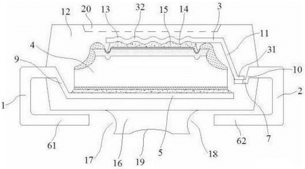
[0019] Embodiment 1: a kind of miniature surface-mounted semiconductor rectifier device, comprises epoxy encapsulation body 12 and the first lead bar 1 that is located in the epoxy encapsulation body 12, the second lead bar 2, connecting piece 3 and diode chip 4, One end of the first lead bar 1 is a support area 5 connected to the diode chip 4, one end of the diode chip 4 is electrically connected to the support area 5 through solder paste, and the other end of the first lead bar 1 is a first pin area 61, The first pin area 61 of the first lead bar 1 serves as the current transmission end of the rectifier;

[0020] One end of the second lead bar 2 is a welding area 7 connected to the first welding end 31 of the connecting piece 3, the other end of the second lead bar 2 is a second pin area 62, and the second lead bar 2 The second pin area 62 is used as the current transmission end of the rectifier; the second welding end 32 of the connecting piece 3 is electrically connected t...

Embodiment 2

[0026] Embodiment 2: A kind of miniature surface-mounted semiconductor rectifier device, comprises the first lead bar 1, the second lead bar 2, the connection piece 3 and the diode chip 4 that are positioned at the epoxy encapsulation body 12, and this first lead bar 1 one end It is the support area 5 connected with the diode chip 4, one end of the diode chip 4 is electrically connected with the support area 5 through solder paste, the other end of the first lead bar 1 is the first pin area 61, the first lead bar 1 The first pin area 61 serves as the current transmission end of the rectifier;

[0027] One end of the second lead bar 2 is a welding area 7 connected to the first welding end 31 of the connecting piece 3, the other end of the second lead bar 2 is a second pin area 62, and the second lead bar 2 The second pin area 62 is used as the current transmission end of the rectifier; the second welding end 32 of the connecting piece 3 is electrically connected to the other en...


PUM

PropertyMeasurementUnit
areaaaaaaaaaaa

Abstract

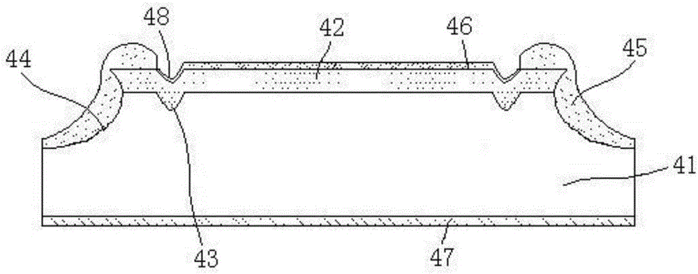
The invention provides a miniature surface mounting semiconductor rectification device. The heavily doped N type zone close to the inner side of an insulation passivation protective layer is provided with a U-shaped slot; the lower surface of the heavily doped N type zone is provided with a downward boss just below the U-shaped slot; the exposed surfaces of the heavily doped N type zone and U-shaped slot are covered by a first metal layer as an electrode; the bottom of an epoxy encapsulation body is provided with a bar-shaped projection insulation part located between the pin zone of a first molded strip and the pin zone of a second molded strip; a first arc concave zone, a second arc concave zone, and a third arc concave zone are respectively located on two side surfaces, and the lower surface of the bar-shaped projection insulation part. According to the invention, a chip area can be reduced to 60-65 mil from 80 mil; under the condition of not influencing an overvoltage protection capability, the cost of a chip can be reduced by 11%, and the welding machine yield of a high power device is more than 97%.

Description

technical field [0001] The invention relates to the field of rectifier devices, in particular to a miniature surface mounted semiconductor rectifier device. Background technique [0002] The miniature surface mount semiconductor rectifier device is an electronic device with unidirectional current conduction. The existing miniature surface mount semiconductor rectifier devices mainly have the following technical problems: On the one hand, the internal material connection method of the device is mainly through solder pads at high temperature. The lower melting connects the chip and the lead firmly together, but it is difficult to achieve 100% fusion of the copper lead and the solder. Usually, the effective welding area of ​​the chip and the connecting piece is 85%, while the end of the lead is only about 60%. When a large current passes, the current distribution is uneven, which reduces the ability of the product to withstand surges. [0003] "Soldering" is a key process in t...

Claims


Application Information

Patent Timeline
Patent Type & Authority Applications(China)
IPC IPC(8): H01L29/86H01L23/498H01L29/06
CPCH01L23/498H01L29/06H01L29/86H01L2924/181H01L2224/32245H01L2924/00012
Inventor 陈伟元
Owner SUZHOU VOCATIONAL UNIV
Learn More