Manufacturing process of leadframe-based BGA packages

Inactive Publication Date: 2009-04-02
CHIPMOS TECH INC
View PDF2 Cites 30 Cited by
  • Summary
  • Abstract
  • Description
  • Claims
  • Application Information

AI Technical Summary

Benefits of technology

[0006]The main purpose of the present invention is to provide a manufacturing process of leadframe-based BGA packages. A leadless leadframe has a two-layer structure. After encapsulation and before jointing solder ball, a half-etching process is performed to remove sacrificial pads of the leadless leadframe and to make the ball pads of the leadless leadframe electrically isolated and embedded in the encapsulant with their bottom surfaces exposed from the encapsulant to define and control the soldering areas of the ball pads without any solder mask. Moreover, bleeding of the solder balls on the ball pads during reflowing can be avoided and the mold flash at the bottom surface of the encapsulant can easily be detected and removed.
[0007]The second purpose of the present invention is to provide a manufacturing process of leadframe-based BGA packages where a leadless leadframe not only has leads and ball pads, but also has a plurality of sacrificial pads in a lower layer aligning and connecting with the ball pads. During the half-etching process, the sacrificial pads are removed to form a plurality of cavities on the bottom of encapsulant which expose the bottom surfaces of the ball pads and are to be filled with solder balls after reflowing to increase the soldering strength of the solder balls.
[0008]The third purpose of the present invention is to provide a manufacturing process of leadframe-based BGA packages where a leadless leadframe further includes a die pad and a plurality of tie bars connecting to the die pad. The tie bars are formed in a lower layer of the leadless leadframe. During the half-etching process, the tie bars are removed along with the leads to prevent solder diffusion under the die pad.
[0009]The manufacturing process of a leadframe-based BGA package according to the present invention is provided. Firstly, a leadless leadframe having an upper layer and a lower layer where a plurality of ball pads are formed in the upper layer and a plurality of sacrificial pads are formed in the lower layer is provided. The sacrificial pads align and connect with the ball pads. The leadless leadframe further includes a plurality of leads in either the lower layer or the upper layer. Then, during a die-attaching step, at least a chip is attached onto the upper layer of the leadless leadframe. During or after the die-attaching step, the chip is electrically connected to the leadless leadframe. Then, during encapsulation, an encapsulant is formed on the leadless leadframe so that the ball pads are embedded inside the encapsulant and the bottom surfaces of the sacrificial pads are exposed from the bottom of the encapsulant. In the half-etching process after encapsulation, the sacrificial pads even with the leads are removed to make the embedded ball pads electrically isolated and their bottom surfaces partially exposed from the encapsulant. Then, a plurality of solder balls are jointed on the ball pads. Therefore, the ball jointing areas of the ball pads can be defined without any solder mask. Moreover, mold flash can easily be detected and removed to enhance the soldering strength of the solder balls at lower cost.

Problems solved by technology

However, the reflow temperature to ensure good wetting of the solder balls may cause unrestrained bleeding of the fused solder to the undesired spots, leading to the insufficient heights of the solder balls or even bridging between the leads.
However, during encapsulation, the leadframes are laid on the molding chest or adhesive tapes with only the protruded soldering areas of the leads in contact with the supporting surfaces of the molding chest or tapes, and mold flashes therefore become an issue.
Moreover, since the soldering areas of the leads and the bottom surface of the encapsulant are on the same plane so that mold flash can not easily be detected and removed leading to weakening soldering strength and dropping of solder balls.
Since there are gaps between the leads, the non-conductive film must be pre-formed in compliance with the layout of the leads where extra costs are incurred due to the application of this additional material.
Once the through holes of the non-conductive film are not completely covered by the leads, encapsulant may flow into the through holes leading to failure of solder ball joint.

Method used


Image

  • Manufacturing process of leadframe-based BGA packages
  • Manufacturing process of leadframe-based BGA packages
  • Manufacturing process of leadframe-based BGA packages

Examples


first embodiment

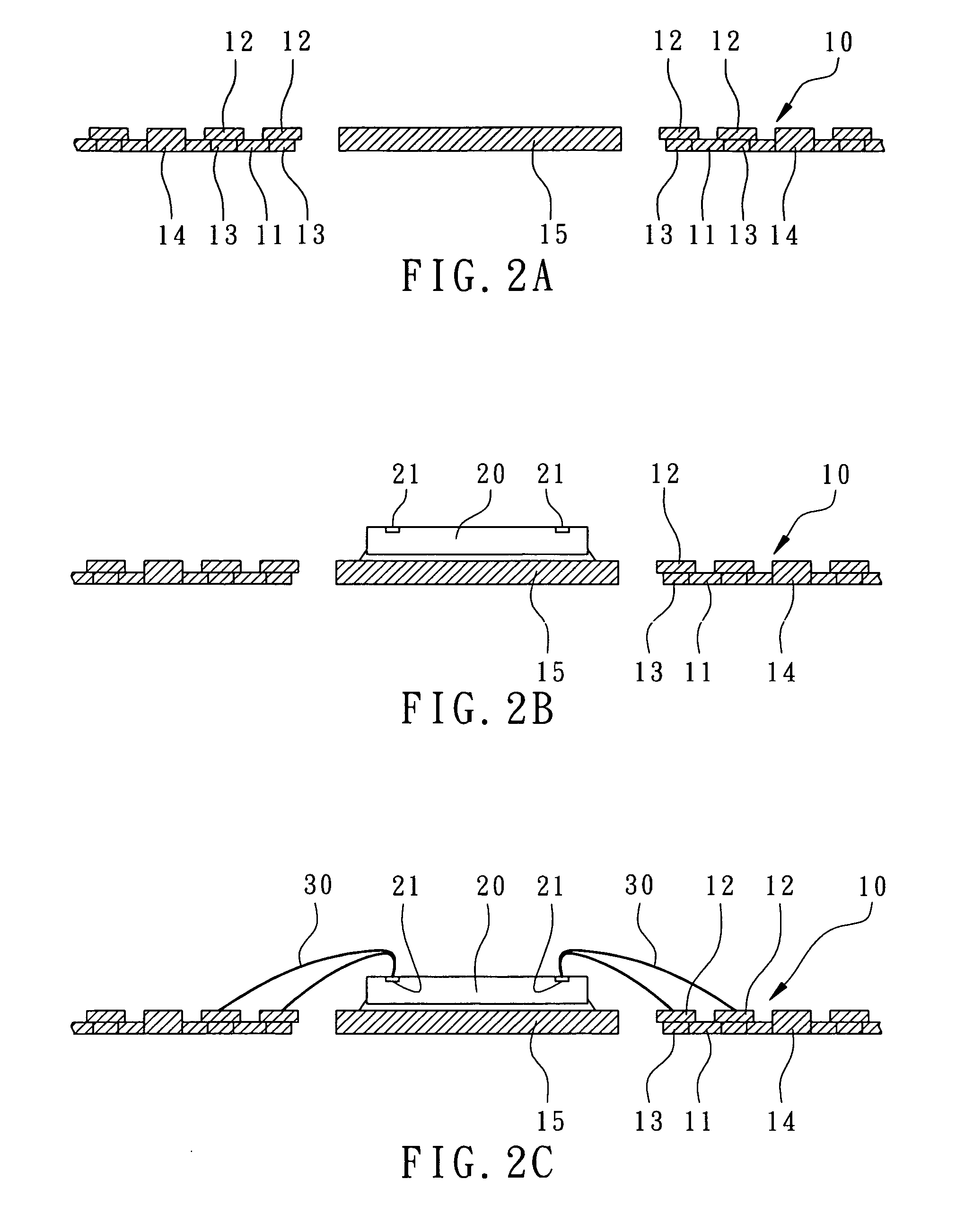
[0019]According to the present invention, firstly, as shown in FIG. 2A, a leadless leadframe 10 with an upper layer and a lower layer is provided where a plurality of arrayed packaging units are defined thereupon to manufacture a plurality of leadframe-based BGA packages. As shown in FIGS. 3 and 4, in each packaging unit, the leadless leadframe 10 includes a plurality of leads 11 and a plurality of ball pads 12. The leads 11 are formed in the lower layer of the leadless leadframe 10. The ball pads 12 are formed in the upper layer of the leadless leadframe 10 and connect with the leads 11 through a plurality of sacrificial pads 13. The leads 11 further connect to the frame bars 14 disposed at the edges of the packaging unit to fix the ball pads 12. Preferably, as shown in FIG. 3, the ball pads 12 are disposed in array and each of the leads 11 connects at least two of the ball pads 12 to achieve a high-density layout of the ball pads 12. As shown in FIG. 2A and FIG. 4, the plurality o...

third embodiment

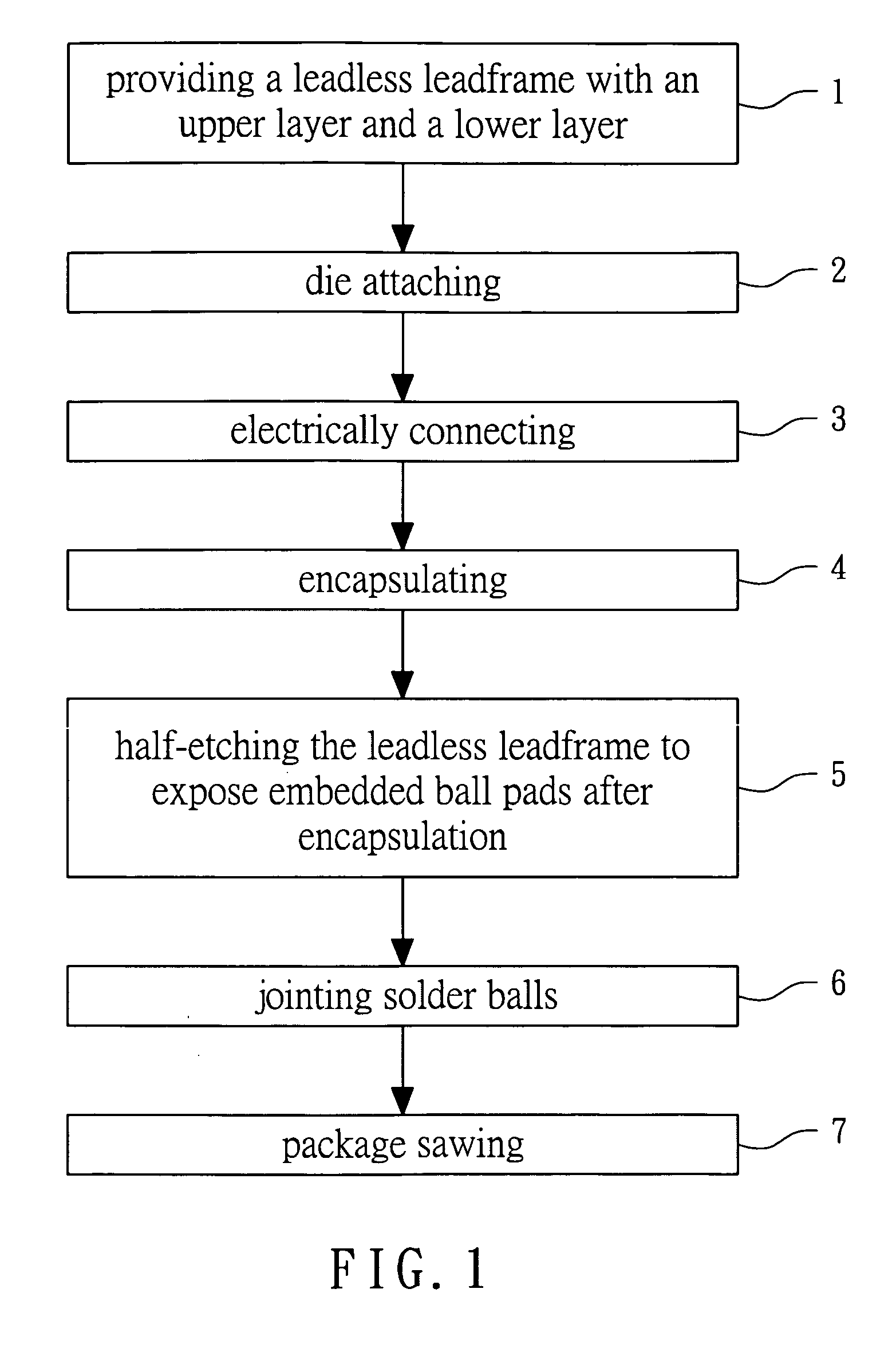
[0028]A manufacturing process of a leadframe-based BGA package is revealed according to the present invention. The primary process includes the steps shown in FIG. 1. The detail descriptions are illustrated with FIG. 7A to FIG. 7H as follows.

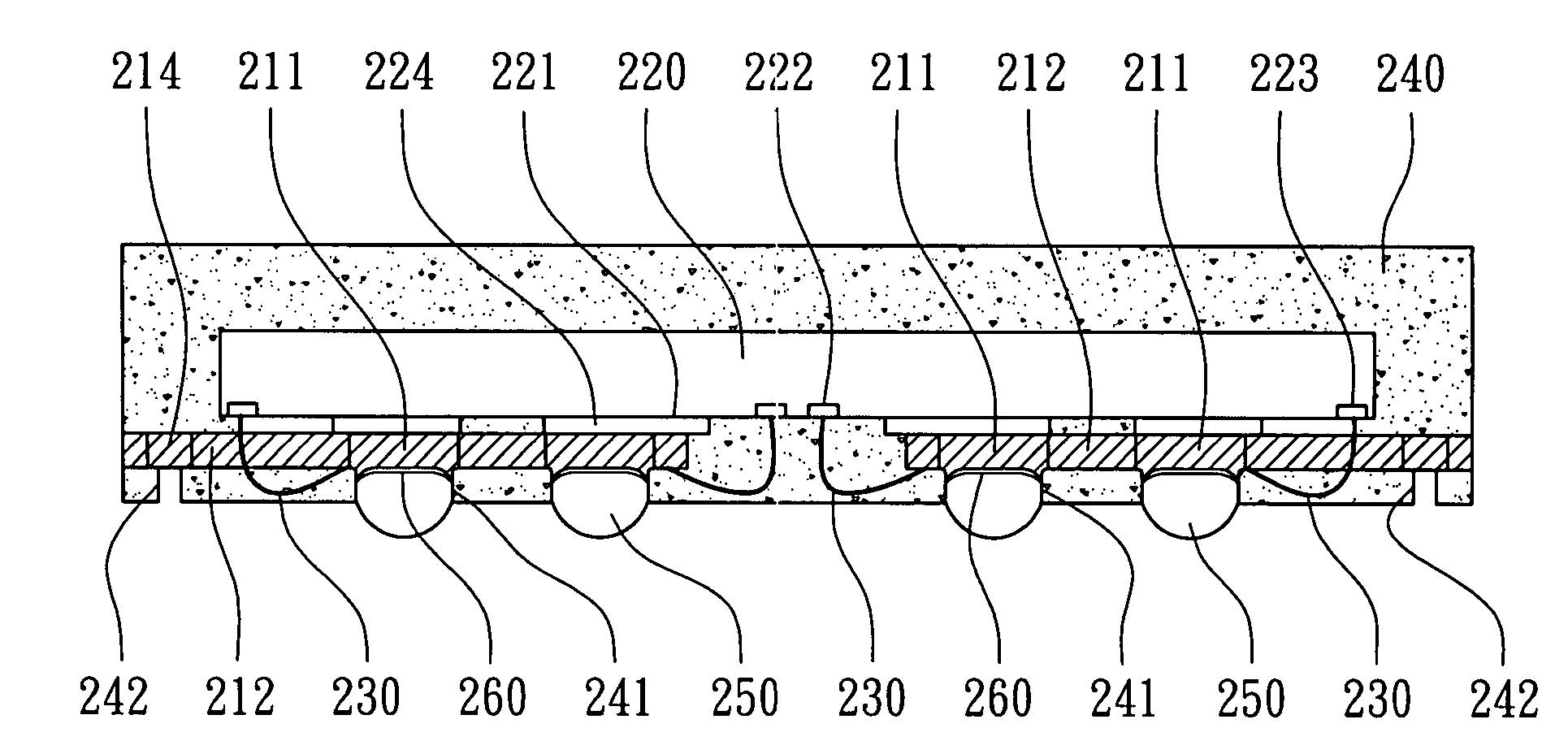
[0029]Firstly, in step 1 as illustrated in FIG. 7A, a leadless leadframe 210 having an upper layer and a lower layer prefabricated by etching processes is provided, where the upper layer includes a plurality of ball pads 211 and a plurality of leads 212 interconnecting the ball pads 211, and the lower layer includes a plurality of sacrificial pads 213 aligning and connecting with the ball pads 211. Normally, the leads 212 are made of metal such as copper, iron, or its alloy. The ball pads 211 and the leads 212 can be formed by a punching or an etching process, and the sacrificial pads 213 are formed by a selective half-etching process on the lower layer of the leadless leadframe 210. To be more specific, the leads 212 are formed in the upper lay...


PUM


Abstract

A manufacturing process of a leadframe-based BGA package is disclosed. A leadless leadframe with an upper layer and a lower layer is provided for the package. The upper layer includes a plurality of ball pads, and the lower layer includes a plurality of sacrificial pads aligning and connecting with the ball pads. A plurality of leads are formed in either the upper layer or the lower layer to interconnect the ball pads or the sacrificial pads. An encapsulant is formed to embed the ball pads after chip attachment and electrical connections. During manufacturing process, a half-etching process is performed after encapsulation to remove the sacrificial pads to make the ball pads electrically isolated and exposed from the encapsulant for solder ball placement where the soldering areas of the ball pads are defined without the need of solder mask(s) to solve the problem of solder bleeding of the solder balls on the leads or the undesired spots during reflow. Moreover, mold flash can easily be detected and removed.

Description

CROSS REFERENCE TO RELATED APPLICATIONS[0001]This is a continuation-in-part of U.S. patent application Ser. No. 11 / 580,310, filed Oct. 13, 2006.FIELD OF THE INVENTION[0002]The present invention relates to fabrication technology of semiconductor devices, and more particularly, to a manufacturing process of leadframe-based BGA (Ball Grid Array) packages.BACKGROUND OF THE INVENTION[0003]Leadframe-based Ball Grid Array (LFBGA) has the advantages of higher packaging density, lower manufacturing cost, and better thermal dissipation. Leadless leadframes replace the traditional printed circuit boards or ceramic substrates with solder balls disposed on the leads of the leadframes. The solder balls are disposed in an array or in multiple rows to provide electrical connections to an external printed circuit board by SMT. Related technologies have been disclosed by R.O.C. Taiwan Patent No. 529770 and 584316.[0004]A reflowing process is required for leadframe-based BGA to solder the solder balls...

Claims


Application Information

Patent Timeline
IPC IPC(8): H01L21/50
CPCH01L21/4828H01L23/3107Y10S438/959Y10S438/94H01L2924/014H01L2924/01322H01L2924/01033H01L2924/01006H01L2924/01005H01L24/48H01L2924/15311H01L2924/01083H01L2924/01082H01L2924/01079H01L2924/01078H01L2924/0105H01L23/4951H01L23/49513H01L23/49534H01L23/49541H01L24/49H01L2224/32245H01L2224/48091H01L2224/48247H01L2224/4826H01L2224/49H01L2224/73215H01L2224/73265H01L2224/92H01L2224/92147H01L2224/92247H01L2924/01028H01L2924/01029H01L2924/01046H01L2924/01047H01L2924/00014H01L2924/00H01L2224/451H01L2224/85207H01L24/45H01L2924/181H01L2924/00012H01L2224/05599
Inventor LIN, HUNG-TSUN
Owner CHIPMOS TECH INC
Why Eureka
Try Eureka