Metal-insulator-metal capacitor structure and fabrication method thereof

A technology of metal capacitors and manufacturing methods, applied in semiconductor/solid-state device manufacturing, semiconductor devices, circuits, etc., can solve the problems of large structure size of MIM capacitors and low requirements on photoresist morphology

Active Publication Date: 2020-06-12
CSMC TECH FAB2 CO LTD
View PDF5 Cites 0 Cited by
  • Summary
  • Abstract
  • Description
  • Claims
  • Application Information

AI Technical Summary

Problems solved by technology

Due to the large size of the MIM capacitor structure in the above applications, the requirements for the shape of the photoresist are not very high

Method used


Image

  • Metal-insulator-metal capacitor structure and fabrication method thereof
  • Metal-insulator-metal capacitor structure and fabrication method thereof
  • Metal-insulator-metal capacitor structure and fabrication method thereof

Examples


Embodiment Construction

[0026] Further description will be given below in conjunction with the accompanying drawings and embodiments.

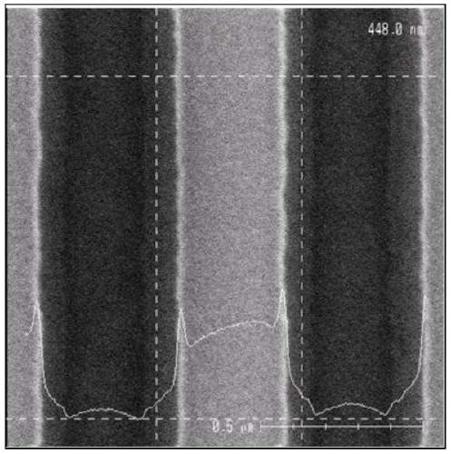
[0027] The method in the following embodiments can be used to fabricate a MIM capacitor ring, the size of which is less than 1 micron. The MIM capacitor ring is a ring-shaped MIM capacitor structure.

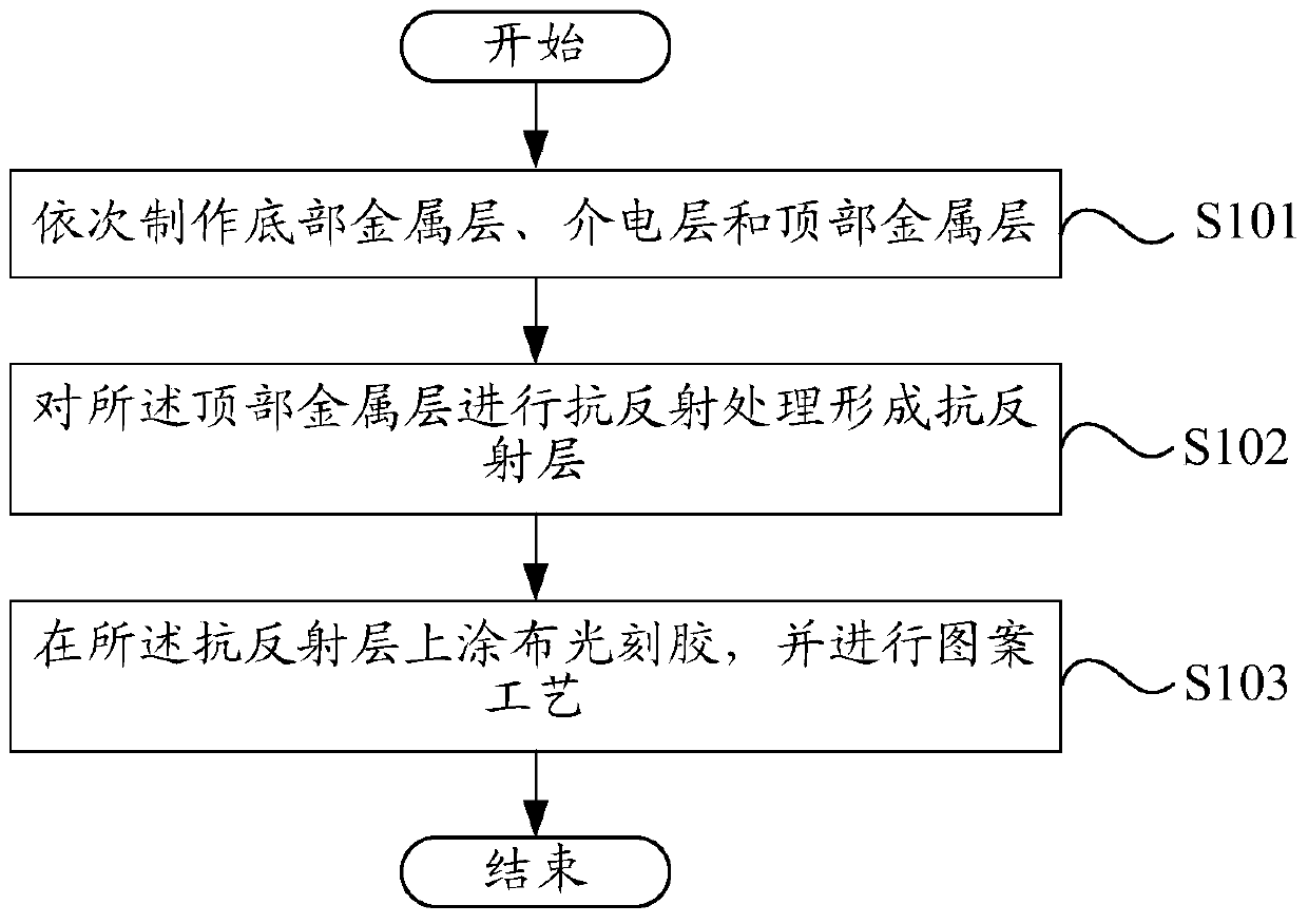
[0028] Such as figure 2 Shown is a flow chart of a fabrication method of a metal-insulator-metal capacitor structure according to an embodiment. The method includes the following steps.

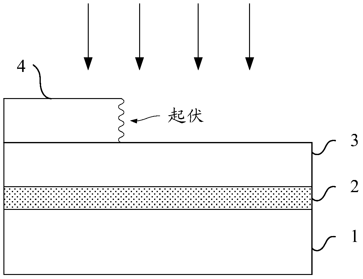
[0029] Step S101 : sequentially fabricate the bottom metal layer 100 , the dielectric layer 200 and the top metal layer 300 . The fabrication process of the bottom metal layer 100 , the dielectric layer 200 and the top metal layer 300 can all adopt a deposition process. Referring to FIG. 3 , the thickness of the bottom metal layer 100 is 3000-5000 angstroms, preferably 4000 angstroms; the thickness of the dielectric layer 200 is 300-400 angstroms, preferably 350 angstroms; the th...


PUM

PropertyMeasurementUnit
thicknessaaaaaaaaaa
thicknessaaaaaaaaaa
thicknessaaaaaaaaaa

Abstract

The invention relates to a manufacturing method of a metal-insulator-metal capacitor structure, which comprises the steps of sequentially manufacturing a bottom metal layer, a dielectric layer and a top metal layer; carrying out anti-reflection processing on the top metal layer so as to form an anti-reflection layer; and coating the anti-reflection layer with photoresist, and carrying out a patterning process. The invention further relates to a metal-insulator-metal capacitor structure applied to the manufacturing method. According to the method and the structure provided by the invention, the top metal layer is subjected to the anti-reflection processing, so that a standing wave effect in exposure can be effectively prevented when the patterning process is carried out, and the side wall profile of the photoresist is enabled to be neat.

Description

technical field [0001] The invention relates to the technical field of integrated circuits, in particular to a metal-insulator-metal capacitor structure and a manufacturing method thereof. Background technique [0002] With the development of circuit manufacturing technology, the integration of circuits is getting higher and higher, and some passive devices, such as capacitors, are gradually incorporated into integrated circuits. Capacitance appears in an integrated circuit as a metal-insulator-metal (Metal-Insulation-Metal, MIM) capacitor structure. The MIM capacitor structure typically includes a stacked bottom electrode, dielectric material, and top electrode. [0003] For the MIM capacitor structure, when the reflectivity of the top electrode is strong, when the photoresist is used to pattern the top metal layer, the exposure of the photoresist is prone to produce a standing wave effect, which will form uneven topography on the side wall of the photoresist. Such as Fi...

Claims


Application Information

Patent Timeline
Patent Type & Authority Patents(China)
IPC IPC(8): H01L21/02H01L29/92
Inventor 高永亮陈辉
Owner CSMC TECH FAB2 CO LTD
Why Eureka
Try Eureka