Cadmium-telluride thin-film solar battery and preparation method thereof
A technology of solar cells and cadmium telluride, which is applied in circuits, photovoltaic power generation, electrical components, etc., can solve the problems of reduced conversion efficiency of cells, performance deterioration of thin-film solar cells, and 2´ performance degradation of transparent conductive layers, etc.
- Summary
- Abstract
- Description
- Claims
- Application Information
AI Technical Summary
Problems solved by technology
Method used
Image


Examples
preparation example Construction
[0033] The invention also discloses a method for preparing a cadmium telluride thin film solar cell, comprising the following steps
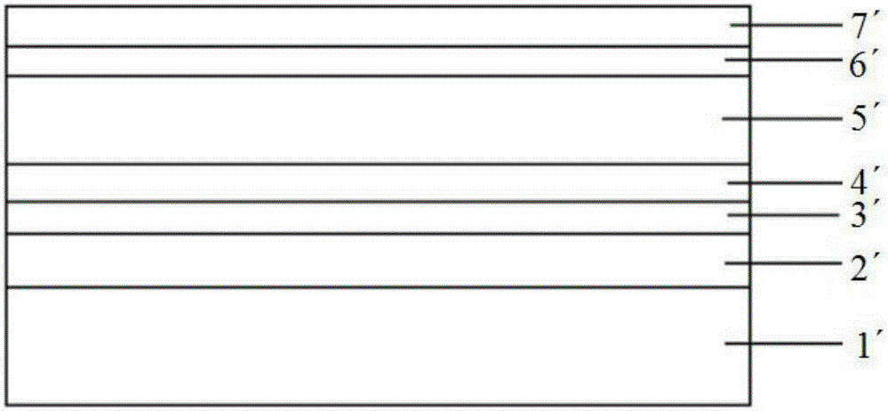
[0034] S1, preparing a glass substrate 1;
[0035] S2, sequentially prepare a laminated structure, transparent conductive layer 2, buffer layer 3, n-type semiconductor layer 4, p-type semiconductor layer 5, back contact layer 6 and back electrode layer on the glass substrate 1 along the direction away from the glass substrate 1 7. The laminate structure includes a suppression layer 8 and a dielectric layer, the suppression layer 8 is prepared on the glass substrate 1, the dielectric layer is prepared between the suppression layer 8 and the transparent conductive layer 2, and the suppression layer 8 contains Si and O elements, and the suppression layer 8 also contains at least one element of Al and B and at least one element of Li and K, and the suppression layer 8 and the dielectric layer have light transmission.
Embodiment 1
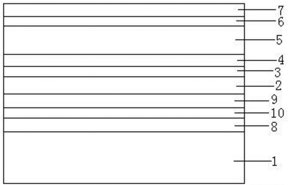
[0038] Form a 35nm suppression layer 8 on the surface of the glass substrate 1, the suppression layer 8 contains Si, O, B, Li elements; then form a 50nm silicon dioxide film layer on the suppression layer 8 as a low refractive index material layer 9 ; Then form a 400nm aluminum-doped zinc oxide film layer on the silicon dioxide film layer 9 as a transparent conductive layer 2; then form a 70nm zinc oxide film layer on the aluminum-doped zinc oxide film layer 2 as a buffer layer 3; then Form the cadmium sulfide film layer of 100nm on the zinc oxide film layer 3 as the n-type semiconductor layer 4; then form the cadmium telluride film layer of 2um on the cadmium sulfide film layer 4 as the p-type semiconductor layer 5; Layer 5 is subjected to cadmium chloride vapor heat treatment; then a 100nm copper-doped cadmium telluride film layer is formed on the cadmium telluride film layer 5 as the back contact layer 6; then a 300nm metal The molybdenum layer serves as the back electrode ...
Embodiment 2
[0041] Form a layer of 40nm suppression layer 8 on the surface of the glass substrate 1, the suppression layer 8 contains Si, O, B, K elements; then form a 60nm silicon dioxide film layer on the suppression layer 8 as a low refractive index material layer 9 ; Then form a 400nm aluminum-doped zinc oxide film layer on the silicon dioxide film layer 9 as a transparent conductive layer 2; then form a 60nm zinc oxide film layer on the aluminum-doped zinc oxide film layer 2 as a buffer layer 3; then Form the cadmium sulfide film layer of 110nm on the zinc oxide film layer 3 as the n-type semiconductor layer 4; then form the cadmium telluride film layer of 2um on the cadmium sulfide film layer 4 as the p-type semiconductor layer 5; Layer 5 is subjected to cadmium chloride vapor heat treatment; then an 80nm copper-doped cadmium telluride film layer is formed on the cadmium telluride film layer 5 as the back contact layer 6; then a 350nm metal The molybdenum layer serves as the back el...
PUM
| Property | Measurement | Unit |
|---|---|---|
| Thickness | aaaaa | aaaaa |
Abstract
Description
Claims
Application Information
 - R&D
- Intellectual Property
- Life Sciences
- Materials
- Tech Scout
- Unparalleled Data Quality
- Higher Quality Content
- 60% Fewer Hallucinations
Browse by: Latest US Patents, China's latest patents, Technical Efficacy Thesaurus, Application Domain, Technology Topic, Popular Technical Reports.
© 2025 PatSnap. All rights reserved.Legal|Privacy policy|Modern Slavery Act Transparency Statement|Sitemap|About US| Contact US: help@patsnap.com