


Quick Research
Generate reliable direction feasibility study reports for your R&D in just a few steps.

Technical Q&A
Discover and master advanced knowledge NOW. Basics, ideas, possibilities, all at once.

Find Solutions
As an expert in R&D theories, this can generate solutions to your technical problems instantly.

Evaluate Feasibility
Analyze your overall solution with one click, know your potential R&D risks in advance.

Monitor Landscape
Get weekly tech updates, stay abreast of the latest tech innovations and key insights.
Band-gag-modified Ge material and preparation method thereof
A technology of modification and substrate material, applied in the direction of polycrystalline material growth, chemical instruments and methods, from chemically reactive gases, etc., can solve problems such as unfavorable alloy growth, improve current drive and frequency characteristics, and reduce manufacturing costs. , The effect of preparation technology is simple
- Summary
- Abstract
- Description
- Claims
- Application Information
AI Technical Summary
Problems solved by technology
Method used
Image

Examples
Embodiment 1
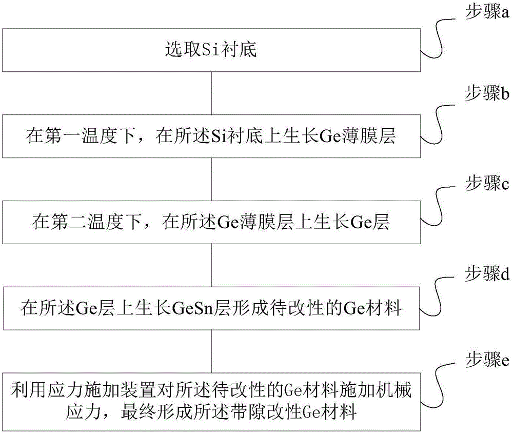
[0051] See figure 1 , figure 1 A flow chart of a method for preparing a direct bandgap Ge material provided in an embodiment of the present invention; the method includes the following steps:
[0052] Step a, select Si substrate;
[0053] Step b, growing a Ge thin film layer on the Si substrate at a first temperature;
[0054] Step c, growing a Ge layer on the Ge thin film layer at a second temperature;
[0055] Step d, growing a GeSn layer on the Ge layer to form a Ge material to be modified;
[0056] Step e, using a stress applying device to apply mechanical stress to the Ge material to be modified to finally form the bandgap modified Ge material.
[0057] Wherein, in step b and step c, the first temperature is lower than the second temperature. That is, relatively speaking, the first temperature is low temperature, and the second temperature is high temperature. For example, the first temperature is 275°C-325°C; the second temperature is 500°C-600°C.
[0058] Optiona...
Embodiment 2
[0074] See Figure 4a-Figure 4d , Figure 4a-Figure 4d It is a schematic diagram of a method for preparing a direct bandgap Ge material provided by an embodiment of the present invention. On the basis of the above embodiments, this embodiment will introduce the process flow of the present invention in more detail. The method includes:
[0075] S101. Substrate selection. Such as Figure 4a As shown, the Si substrate sheet 201 whose crystal orientation is (001) is selected as the original material;
[0076] S102. Growth of epitaxial layer: using molecular beam epitaxy (MBE), grow an n-type Ge thin film with a crystal orientation of (001) on a Si substrate by a two-step method of low temperature and high temperature, with a doping concentration of 1×10 16 ~5×10 16 cm -3 . specifically:
[0077] S1021, such as Figure 4b As shown, a 50nm-thick "low temperature" Ge (LT-Ge) thin film 202 is grown at 275-325°C. Most of the relaxation of elastic stress occurs in the low-temp...
PUM
 Abstract
Description
Claims
Application Information
 - R&D Engineer
- R&D Manager
- IP Professional
- Industry Leading Data Capabilities
- Powerful AI technology
- Patent DNA Extraction
Browse by: Latest US Patents, China's latest patents, Technical Efficacy Thesaurus, Application Domain, Technology Topic, Popular Technical Reports.
© 2024 PatSnap. All rights reserved.Legal|Privacy policy|Modern Slavery Act Transparency Statement|Sitemap|About US| Contact US: help@patsnap.com