
A method for directly epitaxially growing germanium dummy substrate on silicon substrate

An epitaxial growth, silicon substrate technology, applied in electrical components, circuits, semiconductor/solid-state device manufacturing, etc., can solve the problems of unfavorable III-V heterostructure growth, large surface roughness of epitaxial layers, and dislocation density of epitaxial layers. Advanced problems, to achieve the effect of high single crystal quality, low cost and simple preparation process

Active Publication Date: 2021-03-19
NANJING UNIV
View PDF2 Cites 0 Cited by
  • Summary
  • Abstract
  • Description
  • Claims
  • Application Information

AI Technical Summary

Problems solved by technology

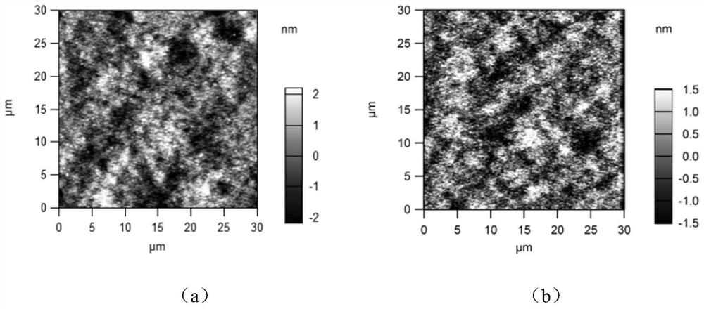
[0005] 1) The surface roughness of the Ge epitaxial layer is large, which is not conducive to the growth of III-V heterostructures on the subsequent Ge buffer layer;
[0006] 2) The high dislocation density of the Ge epitaxial layer degrades the performance of the device when it is applied in optoelectronic devices
This method is complicated to operate and needs to constantly change the ratio of germanium to silicon, which not only wastes time but also costs a lot

Method used


Image

  • A method for directly epitaxially growing germanium dummy substrate on silicon substrate
  • A method for directly epitaxially growing germanium dummy substrate on silicon substrate
  • A method for directly epitaxially growing germanium dummy substrate on silicon substrate

Examples


Embodiment Construction

[0031] The present invention will be described in further detail below in conjunction with the accompanying drawings and specific embodiments.

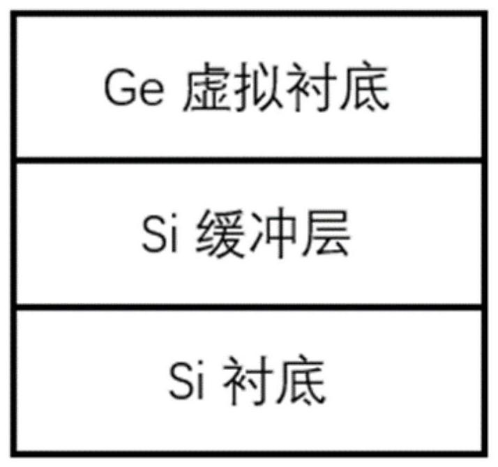
[0032] The invention provides a method for directly epitaxially growing a dummy germanium substrate on a silicon substrate through molecular beam epitaxy. figure 1 It is a structural schematic diagram of the germanium dummy substrate of the present embodiment, and the specific preparation method is as follows:

[0033] Through solid-state source molecular beam epitaxy, the (100) and (111) crystal plane silicon substrates are first surface treated. The silicon substrate treated with hydrofluoric acid is introduced into the vacuum chamber, and the substrate is kept rotating. For the silicon (100) substrate, the substrate heater is raised to 500-600° C. and kept for 5-10 minutes; for the silicon ( 111) Substrate, raising the substrate heater to 800-1000° C. and maintaining it for 5-10 minutes.

[0034] Then a silicon buffer layer with ...


PUM

PropertyMeasurementUnit
thicknessaaaaaaaaaa
surface roughnessaaaaaaaaaa

Abstract

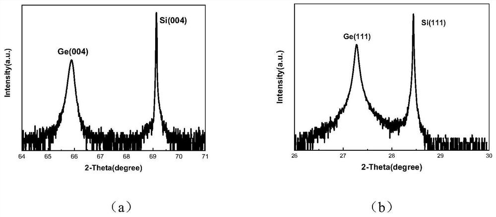
The invention discloses a method for directly epitaxially growing a germanium virtual substrate on a silicon substrate. 1, obtain a silicon substrate of a (100) crystal plane or a silicon substrate ofa (111) crystal plane; 2, aft that silicon substrate is treated with hydrofluoric acid, carry out surface treatment in a vacuum environment; 3, growing a layer of silicon buffer layer on the processed silicon substrate through a molecular beam epitaxy method; Step 4, adjusting to the appropriate growth temperature, and then directly epitaxially growing a germanium virtual substrate with a thickness of micron on the silicon buffer layer. The method of the invention can directly epitaxy the germanium virtual substrate on the silicon wafer, the surface of the germanium virtual substrate grown bythe method is flat, the quality of the single crystal is high, the crystal lattice can be relaxed completely, and the germanium virtual substrate can be used for the growth of subsequent materials instead of the germanium substrate. The method does not need to adopt the layer-by-layer growth mode of gradually increasing the germanium content, and the preparation process is simpler and the cost can be reduced.

Description

technical field [0001] The invention relates to a method for directly epitaxially growing a dummy germanium substrate on a silicon substrate, more specifically, it relates to the optimization of the growth conditions of a dummy substrate of high-quality germanium directly epitaxially grown on a silicon substrate, including the processing of the substrate , the growth of the buffer layer and the optimization process of the growth temperature of the germanium virtual substrate. Background technique [0002] Silicon (Si) and germanium (Ge) are the most common semiconductor materials and are also important materials for electronic components. Silicon-based germanium epitaxial material can be used as a new material for silicon-based high-speed circuit research, and it is the first choice material for silicon-based long-wavelength photodetectors. [0003] In addition, germanium matches the lattice of GaAs materials, and silicon-based germanium epitaxial materials can be used as v...

Claims


Application Information

Patent Timeline
Patent Type & Authority Patents(China)
IPC IPC(8): H01L21/02
CPCH01L21/02381H01L21/02433H01L21/0245H01L21/02532H01L21/02631
Inventor 芦红苗艺魏炼叶佳佳宋欢欢陈延峰
Owner NANJING UNIV
Learn More