N-type ZnO nanorod/p-type diamond ultraviolet photovoltaic detector and preparation method thereof
A diamond and nanorod technology, applied in semiconductor devices, electrical components, circuits, etc., can solve problems such as no testing technology, achieve energy saving, lower requirements, and simple manufacturing process
- Summary
- Abstract
- Description
- Claims
- Application Information
AI Technical Summary
Problems solved by technology
Method used
Image
Examples
Embodiment 1
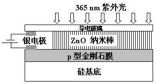
[0037] Example 1: Fabrication of n-type ZnO nanorod / p-type diamond heterojunction ultraviolet photovoltaic detector.
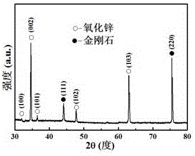
[0038] Boron-doped p-type diamond films were prepared by microwave plasma CVD or hot filament CVD. The substrate for depositing p-type CVD polycrystalline diamond film is a single crystal Si wafer, and hydrogen, oxygen, methane and nitrogen are used as reaction gases. Microwave power 2000W, pressure 7~8kPa, hydrogen flow 100 sccm, oxygen flow 1.5 sccm, nitrogen flow 3 sccm, methane flow 20 sccm, boron source uses borane or trimethyl borate, borane and trimethyl borate are carried in by hydrogen In the reaction chamber, the flow rate is 10~20 sccm, and the substrate temperature is maintained at 1000 o C, the growth time of the film is 3 hours, and a boron-doped p-type CVD polycrystalline diamond film is grown.
Embodiment 2
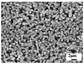
[0039] Example 2: Prepare n-type ZnO nanorods by thermal evaporation, using a high-temperature tubular resistance furnace, place the source material in a small quartz test tube with an open end, an inner diameter of 11 mm, and a length of 20 cm, downstream of the source material Place the substrate. The quartz test tube is placed in a long quartz tube and placed in a fixed position in the tube furnace. In the experiment, a mechanical pump was used to draw a vacuum, and a certain flow of working gas O was introduced. 2 , Ar as the carrier gas. Configure a mixture of ZnO powder and reducing agent metal powder aluminum powder (produced by Tianjin Guangfu Fine Chemical Research Institute, with a purity of 99.99%) at a mass ratio of 1:1 as the evaporation source, grind it fully in a mortar and put it into a quartz test tube Inside, the cleaned substrate is placed in a quartz cuvette downstream of the evaporation source. Place the quartz test tube in the heating zone of the tube ...
Embodiment 3
[0040] Embodiment 3: A kind of method for preparing n-type ZnO / p-type diamond ultraviolet photovoltaic detector by thermal evaporation method is carried out according to the following steps,
[0041] The first step is to grow p-type boron-doped diamond film by using microwave plasma CVD method, using borane as boron source, silicon as substrate, and growing for about 4 hours.
[0042] In the second step, a ZnO nanorod array structure is grown in a high-temperature tubular resistance furnace on the p-type diamond film by thermal evaporation. ZnO and aluminum powder were mixed at a mass ratio of 1:1 as the evaporation source and placed at the bottom of the quartz test tube, and the p-type diamond film was placed downstream of the evaporation source in the quartz tube. Put the quartz test tube into the tube furnace, place the evaporation source in the heating temperature zone of the tube furnace (~850 o C), p-type diamond is located in the growth temperature region (~500 oC ),...
PUM
 Abstract
Description
Claims
Application Information
 - R&D
- Intellectual Property
- Life Sciences
- Materials
- Tech Scout
- Unparalleled Data Quality
- Higher Quality Content
- 60% Fewer Hallucinations
Browse by: Latest US Patents, China's latest patents, Technical Efficacy Thesaurus, Application Domain, Technology Topic, Popular Technical Reports.
© 2025 PatSnap. All rights reserved.Legal|Privacy policy|Modern Slavery Act Transparency Statement|Sitemap|About US| Contact US: help@patsnap.com


