Solar cell and production method therefor
A technology of silicon solar cells and manufacturing methods, applied in circuits, electrical components, photovoltaic power generation, etc., can solve the problems of poor performance of solar cells, inability to obtain diffusion barrier properties, and poor ohmic contact characteristics, etc., and achieve excellent adhesion , reduced reflection, low wiring resistance and low contact resistance
- Summary
- Abstract
- Description
- Claims
- Application Information
AI Technical Summary
Problems solved by technology
Method used
Image
Examples
Embodiment 1
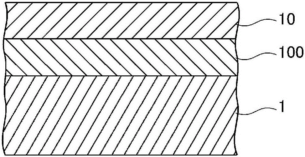
[0153] A single-crystal p-type silicon wafer having a length of 156 mm x a width of 156 mm x a thickness of 0.2 mm was used as the silicon substrate. The p-type impurity is boron (B), and the impurity concentration is about 1×10 16 cm -3 . The upper surface of the wafer was etched with a KOH solution to form a concave-convex texture. Next, coat the upper surface with POCl 3, and then heat treatment at high temperature to diffuse phosphorus (P) in silicon to form n+ regions. The maximum concentration of P is about 1×10 19 cm -3 . As described above, a silicon substrate having an n-p junction was produced.
[0154] As a raw material solution, a mixed solution containing a Ti-based alkoxide compound, an Nb-based alkoxide compound, and a solvent was prepared. Using a slit coater, the raw material solution was evenly coated on the silicon substrate. The coated substrate is dried at about 200°C, and then fired at 600°C for 10 minutes in an atmospheric pressure atmosphere co...
Embodiment 2
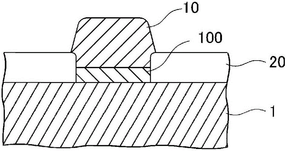
[0170] Using the silicon substrate having an n-p junction of Example 1, an 80-nm-thick SiN film for antireflection was formed on the surface of the substrate by plasma chemical vapor deposition (PECVD). Then, the portion where the copper wiring is formed is removed by laser ablation.
[0171] On the above-mentioned silicon substrate on which the antireflection film was formed, under the same conditions as in Example 1, formation of a metal oxide and formation of copper wiring were carried out.
[0172] The resistivity of the copper wiring was 3.3 μΩcm, the adhesion strength of the copper wiring was 1.9 N / mm, and the visible light transmittance at a wavelength of 500 nm of the metal oxide layer was 92%. In addition, after heat treatment at 500° C. for 30 minutes, copper atoms were below the detection limit, no interdiffusion of Cu and Si was observed, and the diffusion barrier property was good.
Embodiment 3
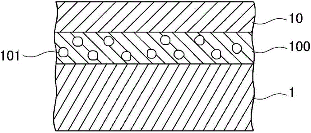
[0174] Under the same conditions as in Example 1, a metal oxide layer comprising copper, titanium, and niobium is formed on a silicon substrate with a thickness of about 30 nm, and then in a reducing atmosphere formed by mixing 5% hydrogen in nitrogen, the The pressure of the atmosphere is 10 4 The heat treatment was performed for 10 minutes under the conditions of Pa and a temperature of 500°C. In the heat-treated structure, copper particles were precipitated in metal oxides containing titanium and niobium. The average diameter of the copper particles is about 5 nm.
[0175] Then, copper wiring was formed by the method described in Example 1. The resistivity of the copper wiring was 3.0 μΩcm, the adhesion strength of the copper wiring was 4.2 N / mm, and the visible light transmittance at a wavelength of 500 nm of the metal oxide layer was 90%. In addition, after heat treatment at 500° C. for 30 minutes, the copper atoms were below the detection limit, no interdiffusion of C...
PUM
| Property | Measurement | Unit |
|---|---|---|
| particle diameter | aaaaa | aaaaa |
| visible light transmittance | aaaaa | aaaaa |
| peel strength | aaaaa | aaaaa |
Abstract
Description
Claims
Application Information
 - R&D
- Intellectual Property
- Life Sciences
- Materials
- Tech Scout
- Unparalleled Data Quality
- Higher Quality Content
- 60% Fewer Hallucinations
Browse by: Latest US Patents, China's latest patents, Technical Efficacy Thesaurus, Application Domain, Technology Topic, Popular Technical Reports.
© 2025 PatSnap. All rights reserved.Legal|Privacy policy|Modern Slavery Act Transparency Statement|Sitemap|About US| Contact US: help@patsnap.com


