Optimizing the Properties of Transparent Conductive Thin Films by Ultrasonic Transducer Coupled with Laser Irradiation
A transparent conductive film, laser irradiation technology, applied in circuits, electrical components, semiconductor devices, etc., can solve the problems of harsh conditions, small performance optimization parameter range, etc., to achieve easy operation, widen the parameter range, and reduce laser irradiation conditions. Effect
- Summary
- Abstract
- Description
- Claims
- Application Information
AI Technical Summary
Problems solved by technology
Method used
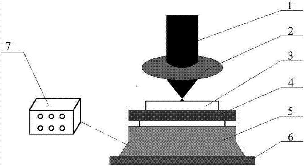
Image

Examples
Embodiment 1
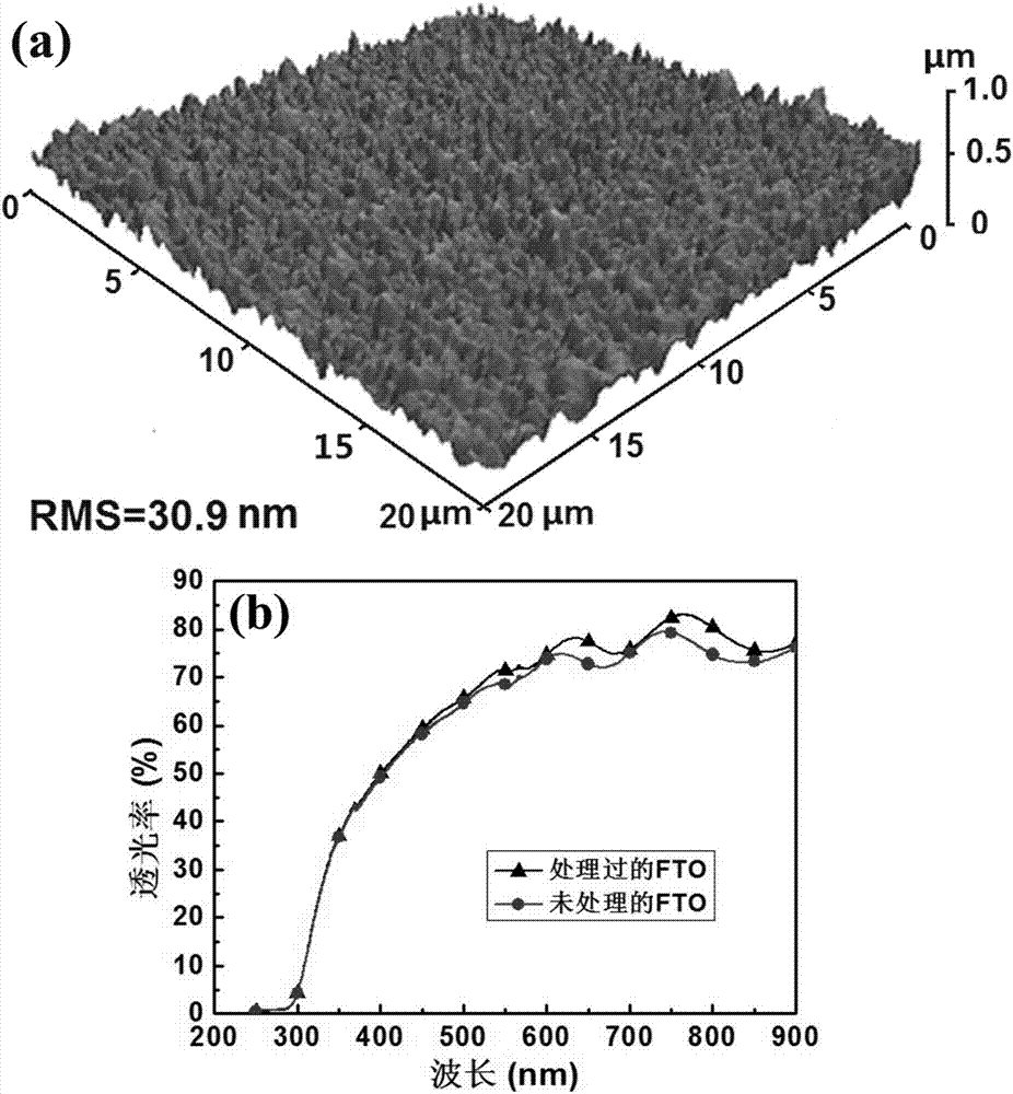
[0035] Embodiment 1: the power of the ultrasonic transducer that this embodiment selects is 100W, and frequency is 10kHz; The pulse width of the nanosecond pulse laser that adopts is 5~8ns, and wavelength is 355nm, and average power is 1.6W (for laser itself Intrinsic parameters, not adjustable), the laser pulse repetition frequency is 10Hz. Fix the pre-cleaned sample on the sample stage, adjust the laser workbench so that the surface of the FTO film sample is located at 0.5mm after the focus of the laser beam; control the energy density of the laser to 0.1J / cm 2 ; start the laser, make the laser beam perpendicular to the surface of the FTO film sample for large-scale scanning, to ensure that the spot overlap rate is 30%, and the scanning line overlap rate is 95%. The surface roughness of the untreated FTO film is 42.3 nm. figure 2 (a) is the AFM image of the FTO film after ultrasonic transduction coupling ultrashort pulse laser irradiation, the surface roughness is 30.9nm, ...
Embodiment 2
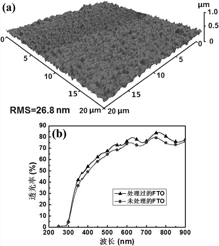
[0036] Embodiment 2: The power of the ultrasonic transducer selected in this embodiment is 300W, and the frequency is 40kHz; Intrinsic parameters, not adjustable), the laser pulse repetition frequency is 1kHz. Fix the pre-cleaned sample on the sample stage, adjust the laser workbench so that the surface of the FTO film sample is located at 2.0mm behind the focus of the laser beam; control the energy density of the laser to 0.4J / cm 2 ; start the laser, make the laser beam perpendicular to the surface of the FTO film sample for large-scale scanning, to ensure that the spot overlap rate is 90%, and the scanning line overlap rate is 80%. The surface roughness of the untreated FTO film is 42.3 nm. image 3 (a) is the AFM image of the FTO film after ultrasonic transduction coupling ultrashort pulse laser irradiation, and its surface roughness is 26.8nm, which is much lower than that before treatment, and the surface density of the film is also significantly improved; image 3 (b) ...
Embodiment 3
[0037] Embodiment 3: the power of the ultrasonic transducer selected in this embodiment is 600W, and frequency is 50kHz; The pulse width of the femtosecond pulsed laser that adopts is 130fs, and wavelength is 800nm, and average power is 2.5W (being the inherent parameter of laser device itself , not adjustable), the laser pulse repetition frequency is 1kHz. Fix the pre-cleaned sample on the sample stage, adjust the laser workbench so that the surface of the AZO film sample is located at 2.5mm after the focus of the laser beam; control the energy density of the laser to 0.8J / cm 2 ; Start the laser, make the laser beam perpendicular to the surface of the AZO film sample for large-area scanning, to ensure that the spot overlap rate is 60%, and the scanning line overlap rate is 60%. The surface roughness of the untreated AZO film was 37.2 nm. Figure 4 (a) is the AFM image of the AZO thin film after ultrasonic transduction coupling ultrashort pulse laser irradiation, its surface ...
PUM
 Abstract
Description
Claims
Application Information
 - R&D
- Intellectual Property
- Life Sciences
- Materials
- Tech Scout
- Unparalleled Data Quality
- Higher Quality Content
- 60% Fewer Hallucinations
Browse by: Latest US Patents, China's latest patents, Technical Efficacy Thesaurus, Application Domain, Technology Topic, Popular Technical Reports.
© 2025 PatSnap. All rights reserved.Legal|Privacy policy|Modern Slavery Act Transparency Statement|Sitemap|About US| Contact US: help@patsnap.com