Matrix and welding method for matrix and diamond piece
A technology of diamond sheet and welding method, which is applied in the field of surface processing and coating, can solve problems such as cracking, large stress, and scrapping, and achieve the effects of good thermal conductivity, low friction coefficient, and good wear resistance
- Summary
- Abstract
- Description
- Claims
- Application Information
AI Technical Summary
Problems solved by technology
Method used
Image
Examples
Embodiment 1
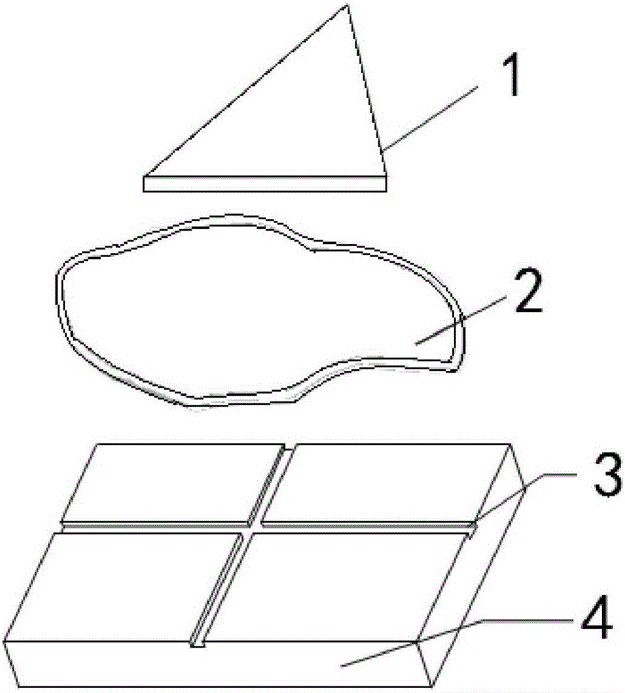
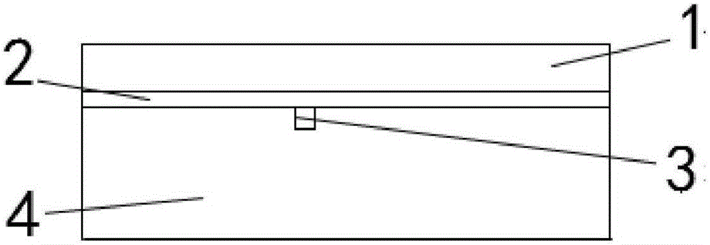
[0020] Embodiment 1: as figure 1 , figure 2 As shown, a substrate, the substrate 4 has a cross groove 3, the cross groove 3 has notches on the side of the substrate 4; the cross groove 3 has notches on the four sides of the substrate 4.
[0021] The cross section of the cross groove 3 is rectangular, V-shaped or arc-shaped.
[0022] The diamond sheet 1 is connected to the substrate 4 through the solder paste 2 , and the cross groove 3 is located under the diamond sheet 1 . The material of the diamond sheet 1 can be diamond single crystal, CVD diamond thick film, polycrystalline diamond, or a composite of CVD diamond thick film and hard alloy, or a composite of polycrystalline diamond and hard alloy.
Embodiment 2
[0023] Embodiment 2: as figure 1 , figure 2 as shown,
[0024] A method for welding a substrate and a diamond sheet, comprising the following steps;
[0025] Mill the cross groove 3 on the surface of the substrate 4 of the cemented carbide, the width of the cross groove 3 is 0.05mm, and the depth of the cross groove 3 is 0.1mm, the surface of the substrate 4 of the cemented carbide is coated with the solder paste 2 of silver-copper-titanium alloy, and the diamond sheet The CVD diamond thick film of 1 is pressed on the solder paste 2, fixed well, after drying, put it into a vacuum brazing furnace to raise the temperature to 800 degrees, keep it warm for 3 minutes, and then cool it down. The material of the diamond sheet 1 can be diamond single crystal, CVD diamond thick film, polycrystalline diamond, or a composite of CVD diamond thick film and hard alloy, or a composite of polycrystalline diamond and hard alloy.
Embodiment 3
[0026] Embodiment 3: as figure 1 , figure 2 Shown, a kind of welding method of substrate and CVD diamond thick film tool;
[0027] The steps are as follows: Mill a cross groove 3 on the surface 4 of a hard alloy with a groove width of 1.8mm and a groove depth of 1.9mm, or process an annular groove plus a cross groove, the annular groove width is 2.0mm, and the annular groove depth is 1.9mm. The surface of the high-quality alloy 4 is covered with silver-copper-titanium alloy solder paste 2, and the CVD diamond thick film of the diamond sheet 1 is pressed on the solder paste to fix it. After drying, put it into a vacuum brazing furnace to raise the temperature to 880 degrees, keep it warm for 3 minutes, and cool down. That's it. The material of the diamond sheet 1 can be diamond single crystal, CVD diamond thick film, polycrystalline diamond, or a composite of CVD diamond thick film and hard alloy, or a composite of polycrystalline diamond and hard alloy.
PUM
| Property | Measurement | Unit |
|---|---|---|
| Vickers hardness | aaaaa | aaaaa |
Abstract
Description
Claims
Application Information
 - Generate Ideas
- Intellectual Property
- Life Sciences
- Materials
- Tech Scout
- Unparalleled Data Quality
- Higher Quality Content
- 60% Fewer Hallucinations
Browse by: Latest US Patents, China's latest patents, Technical Efficacy Thesaurus, Application Domain, Technology Topic, Popular Technical Reports.
© 2025 PatSnap. All rights reserved.Legal|Privacy policy|Modern Slavery Act Transparency Statement|Sitemap|About US| Contact US: help@patsnap.com


