Fabrication method of field-effect transistor and field-effect transistor fabricated by employing fabrication method

A technology of field effect transistors and electrofluids, which is applied in the field of preparation of field effect transistors and the fields of field effect transistors prepared by using them, can solve the problems of self-alignment of gate electrodes and source and drain electrodes, easy destruction of semiconductor active layers, and transistor conductivity Influence and other issues, to achieve the effect of simplifying processing steps, improving electrical performance, and low cost

Active Publication Date: 2016-07-06
HUAZHONG UNIV OF SCI & TECH
View PDF3 Cites 8 Cited by
  • Summary
  • Abstract
  • Description
  • Claims
  • Application Information

AI Technical Summary

Problems solved by technology

[0005] The above-mentioned method of using electrofluidic technology to print micro-nano fibers to prepare transistor channels has the advantages of high resolution, low cost, and simple steps. However, this method requires the process of eliminating or dissolving the fibers. For the top contact When the fiber is removed, the transistor with the structure is particularly easy to damage the semiconductor active layer, which affects the conductivity of the transistor; in addition, the field effect transistor prepared in the above method cannot realize the self-alignment of the gate electrode and the source-drain electrode, which will cause the gate - The parasitic capacitance between the source electrodes and the gate-drain electrodes is too large, which deteriorates the high-frequency characteristics of the device

Method used


Image

  • Fabrication method of field-effect transistor and field-effect transistor fabricated by employing fabrication method
  • Fabrication method of field-effect transistor and field-effect transistor fabricated by employing fabrication method
  • Fabrication method of field-effect transistor and field-effect transistor fabricated by employing fabrication method

Examples


Embodiment Construction

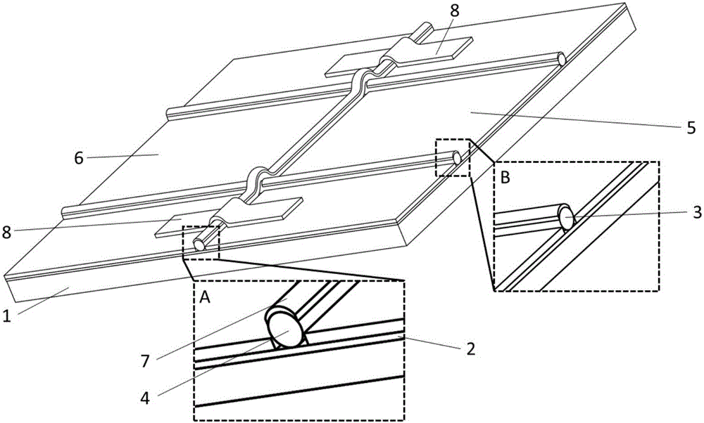
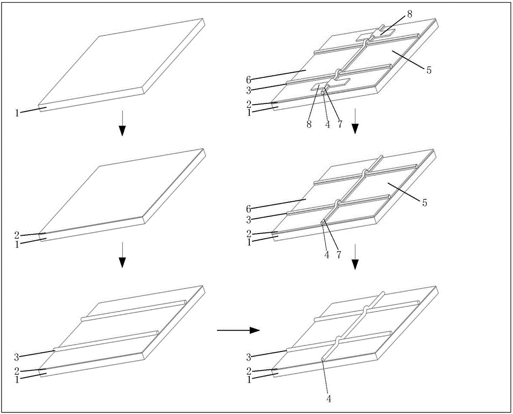
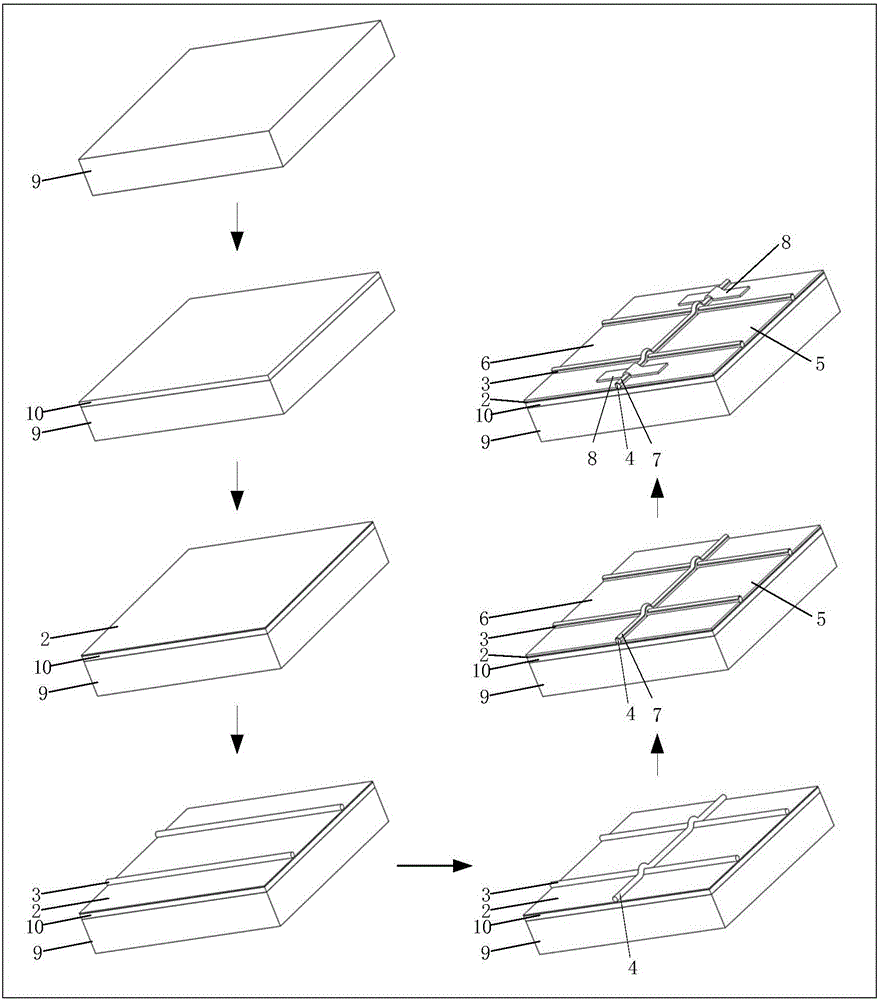
[0033] In order to make the object, technical solution and advantages of the present invention clearer, the present invention will be further described in detail below in conjunction with the accompanying drawings and embodiments. It should be understood that the specific embodiments described here are only used to explain the present invention, not to limit the present invention. In addition, the technical features involved in the various embodiments of the present invention described below can be combined with each other as long as they do not constitute a conflict with each other.

[0034] The preparation method of the field effect transistor of an embodiment of the present invention comprises the following steps:

[0035] 1) Prepare an organic semiconductor thin film on a substrate.

[0036] The substrate can be a rigid substrate or a flexible substrate, and the flexible substrate in this embodiment can be a polyimide film (PI) or a polyethylene terephthalate film (PET), ...


PUM

PropertyMeasurementUnit
thicknessaaaaaaaaaa
diameteraaaaaaaaaa
diameteraaaaaaaaaa

Abstract

The invention discloses a method for fabricating a field-effect transistor by employing an electric fluid direct-writing process. The method comprises the following steps of (1) fabricating an organic semiconductor thin film on a substrate; (2) fabricating linear fibers in parallel on the substrate with the semiconductor thin film by using the electric fluid direct-writing process; (3) fabricating parallel dielectric fibers perpendicular to the linear fibers by electric fluid direct writing; (4) vacuum-depositing metal on the substrate; and (5) applying conductive sliver paste onto the two ends of the dielectric fibers, and leading out a grid electrode. The invention also discloses a corresponding product. According to the method, a transistor channel is obtained by means of the dielectric micro-nano fibers, the length side of the channel is equivalent to the diameter sizes of the fibers and can reach sub-micron even nanoscale, and meanwhile, the fibers are also an insulation layer of the transistor; and moreover, through one-time metal vacuum deposition, a source, a drain and a grid of the field-effect transistor can be simultaneously formed. By the method, the fabrication process step of the transistor is greatly simplified, and meanwhile, the fabrication cost is reduced.

Description

technical field [0001] The invention relates to a preparation method of a field effect transistor and a field effect transistor prepared by using the method. Background technique [0002] Field Effect Transistor (FET) is an active device that uses an electric field to control the conductivity of semiconductor materials. It is one of the most widely used devices in modern electronics. Fields play an irreplaceable role. [0003] In order to be more suitable for integrated circuits and improve the electrical performance of field effect transistors, the length of the transistor channel needs to be effectively controlled, and the process of manufacturing micro-nano-level semiconductor channels with high efficiency, high precision and low cost has attracted much attention. Traditional methods of manufacturing transistor channels include photolithography and nanoimprinting. Among them, photolithography requires high-precision masks, which are costly and complicated; nanoimprinting...

Claims


Application Information

Patent Timeline
Patent Type & Authority Applications(China)
IPC IPC(8): H01L51/40H01L51/05
CPCH10K10/46H10K10/468H10K10/471
Inventor 黄永安江海霞丁亚江
Owner HUAZHONG UNIV OF SCI & TECH
Why Eureka
Try Eureka