Method for fabricating micro-inductors based on 3D printing
A 3D printing, micro-inductance technology, applied in the direction of inductors, circuits, additive manufacturing, etc., can solve the problems of complex processing technology, difficult processing of ferromagnetic materials, difficult IC technology, etc. The incompatibility of materials and semiconductor processes, the effect of reducing the difficulty of preparation and processing
- Summary
- Abstract
- Description
- Claims
- Application Information
AI Technical Summary
Problems solved by technology
Method used
Image

Examples
Embodiment 1
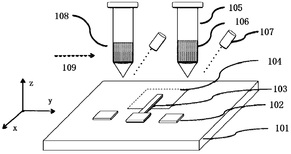
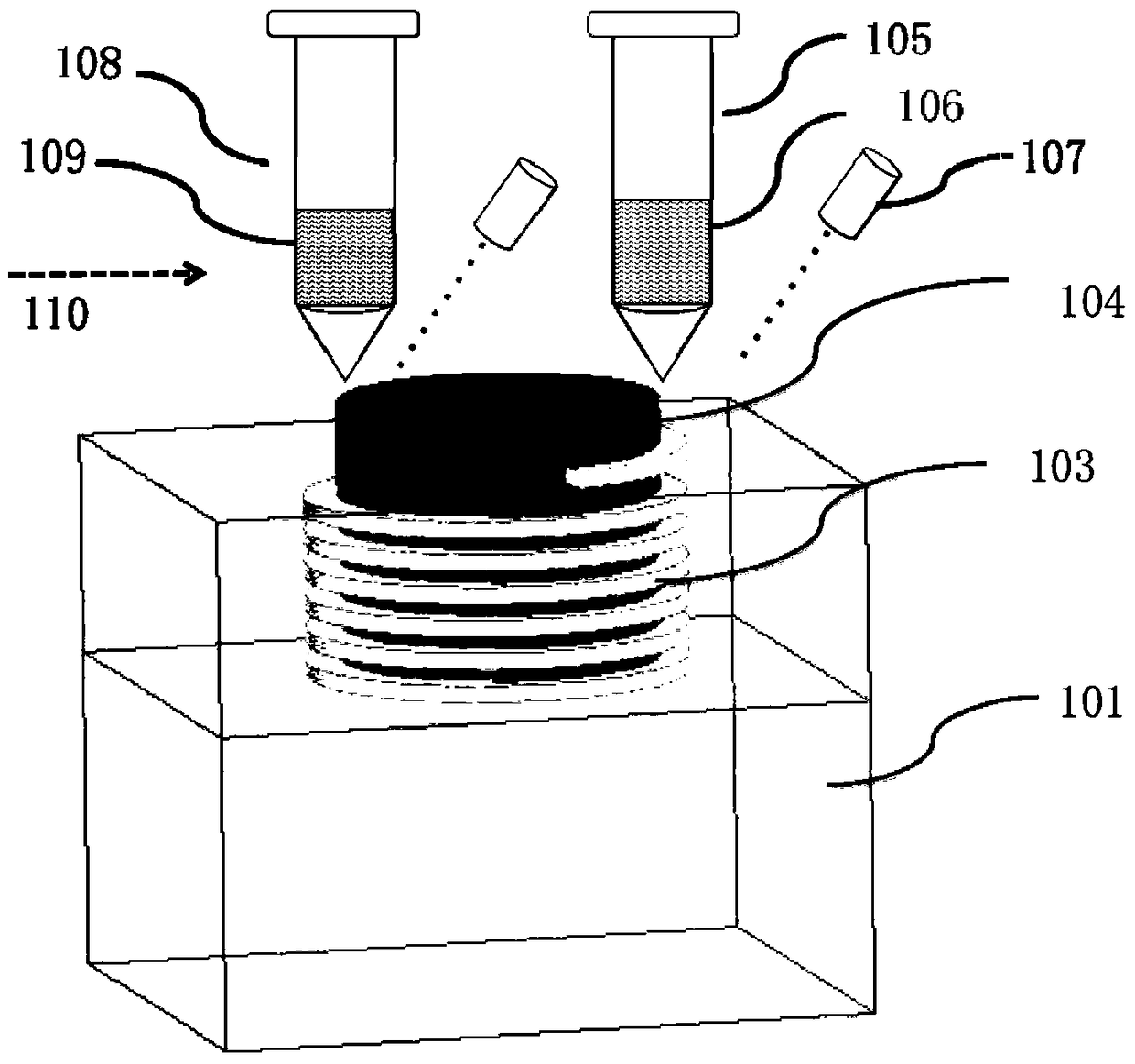
[0053] In this embodiment, the prepared micro-inductance coil is a three-dimensional spiral inductor. The three-dimensional spiral inductor prepared based on 3D printing in this embodiment is as follows: figure 2 shown. Among them, 101 is the substrate for processing the micro-inductor, 103 is the coil of the micro-inductor, 104 is the area for 3D printing ferromagnetic materials, 105 and 108 are the nozzles for 3D printing the micro-inductance coil, 106 and 109 are Cu powder and iron for the micro-inductance coil Magnetic material powder; 107 is the laser required for processing, and 110 is the direction of applying an external magnetic field while printing the magnetic material.
[0054] The diameter of the three-dimensional spiral micro-inductance coil in this embodiment is 100 μm, the coil diameter is 8 μm, the distance between coil layers is 20 μm, and the number of coil layers is 10.
[0055] The preparation method of the present embodiment comprises the following step...
Embodiment 2
[0065] In this embodiment, the micro-inductance coil is a planar micro-inductor. The preparation method comprises the following steps:
[0066] 1) First deposit 500nm SiO on a high-resistance Si substrate 2 film;
[0067] 2) Then use electron beam evaporation to deposit 200nmTi / Au as a buffer layer and bottom electrode to improve the combination of the micro-inductance coil and the substrate;
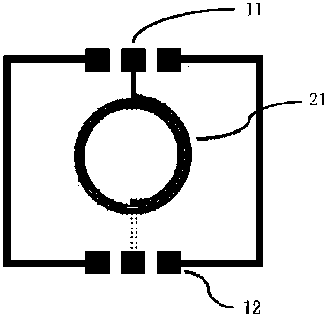
[0068] 3) Then deposit 3 μm metal Cu as the metal material of the micro-inductance coil, and use the MEMS process to process the metal Cu film into a micro-inductance coil 21 and an electrode 11, the electrode size is 300um*500um, the outer diameter of the coil is 500 μm, and the coil width is 15 μm. The pitch between the coils was 25 μm, and the number of coils was 4 turns. Such as image 3 shown.
[0069] 4) Use the 3D printing nozzle to print the ferromagnetic material NiZnCuFeO in the upper area of the micro-inductance coil, with a thickness of 500nm. Oxygen material is crys...
Embodiment 3
[0073] In this embodiment, the micro-inductance coil is a planar micro-inductor. The preparation method comprises the following steps:
[0074] 1) First thermally oxidize the high-resistance Si substrate, and deposit 500nm SiO on the substrate surface 2 film;
[0075] 2) Then use electron beam evaporation to deposit 200nmTi / Au as a buffer layer and a seed layer to improve the combination of the micro-inductance coil and the substrate;
[0076] 3) Then use PECVD to grow an insulating layer SiO with a thickness of 500nm 2 , again using photolithography and dry etching on insulating SiO 2A through hole with a size of 20um*20um is formed on the top;
[0077] 4) Again using magnetron sputtering on SiO 2 500nm Ti / Au is grown on the insulating layer as a through hole to connect the upper and lower electrodes;
[0078] 5) Subsequently, deposit a 3 μm metal Cu metal material film layer on the sample made in step 5), and use the MEMS process to process the metal Cu film layer into...
PUM
| Property | Measurement | Unit |
|---|---|---|
| thickness | aaaaa | aaaaa |
| diameter | aaaaa | aaaaa |
| diameter | aaaaa | aaaaa |
Abstract
Description
Claims
Application Information
 - R&D
- Intellectual Property
- Life Sciences
- Materials
- Tech Scout
- Unparalleled Data Quality
- Higher Quality Content
- 60% Fewer Hallucinations
Browse by: Latest US Patents, China's latest patents, Technical Efficacy Thesaurus, Application Domain, Technology Topic, Popular Technical Reports.
© 2025 PatSnap. All rights reserved.Legal|Privacy policy|Modern Slavery Act Transparency Statement|Sitemap|About US| Contact US: help@patsnap.com