All-graphene family flexible organic field effect tube and manufacturing method thereof

A graphene and organic field technology, which is applied in the direction of graphene, semiconductor/solid-state device manufacturing, photovoltaic power generation, etc., can solve the problems of poor device stability, high requirements for production equipment and process control, and high energy consumption, and achieve the goal of production equipment The effect of low requirements, stable electrical performance, and low material cost

Inactive Publication Date: 2018-07-20
CHINA JILIANG UNIV
View PDF9 Cites 0 Cited by
  • Summary
  • Abstract
  • Description
  • Claims
  • Application Information

AI Technical Summary

Problems solved by technology

At present, the organic semiconductor material with the highest mobility is pentacene. The performance parameters of field effect transistors prepared with this material have reached the level of amorphous silicon. However, the field effect transistors prepared from this material need to be grown by physical vapor deposition under high vacuum. Single crystal thin film is formed, but the growth of single crystal thin film is difficult to control. At the same time, the stability of the device is poor, and it is difficult to meet the production requirements for product yield. Moreover, the physical vapor deposition method requires high vacuum and high temperature, which is harmful to production equipment and High process control requirements and high energy consumption are not conducive to low-cost commercial production; in addition, the current method of preparing flexible electrodes in field effect transistors is to sputter indium tin oxide (ITO) on flexible substrates, but ITO itself is relatively Brittle, it will crack under mechanical stress and excessive bending, so ITO electrodes also restrict the application of device flexibility

Method used


Image

  • All-graphene family flexible organic field effect tube and manufacturing method thereof
  • All-graphene family flexible organic field effect tube and manufacturing method thereof
  • All-graphene family flexible organic field effect tube and manufacturing method thereof

Examples


Embodiment Construction

[0045] In order to make the technical solutions and advantages of the present invention clearer, the present invention will be further described below in conjunction with specific embodiments and with reference to the accompanying drawings.

[0046] The implementation scheme of the field effect transistor with the bottom gate top contact structure is as follows:

[0047] step 1

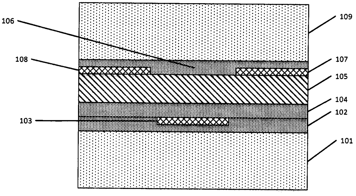
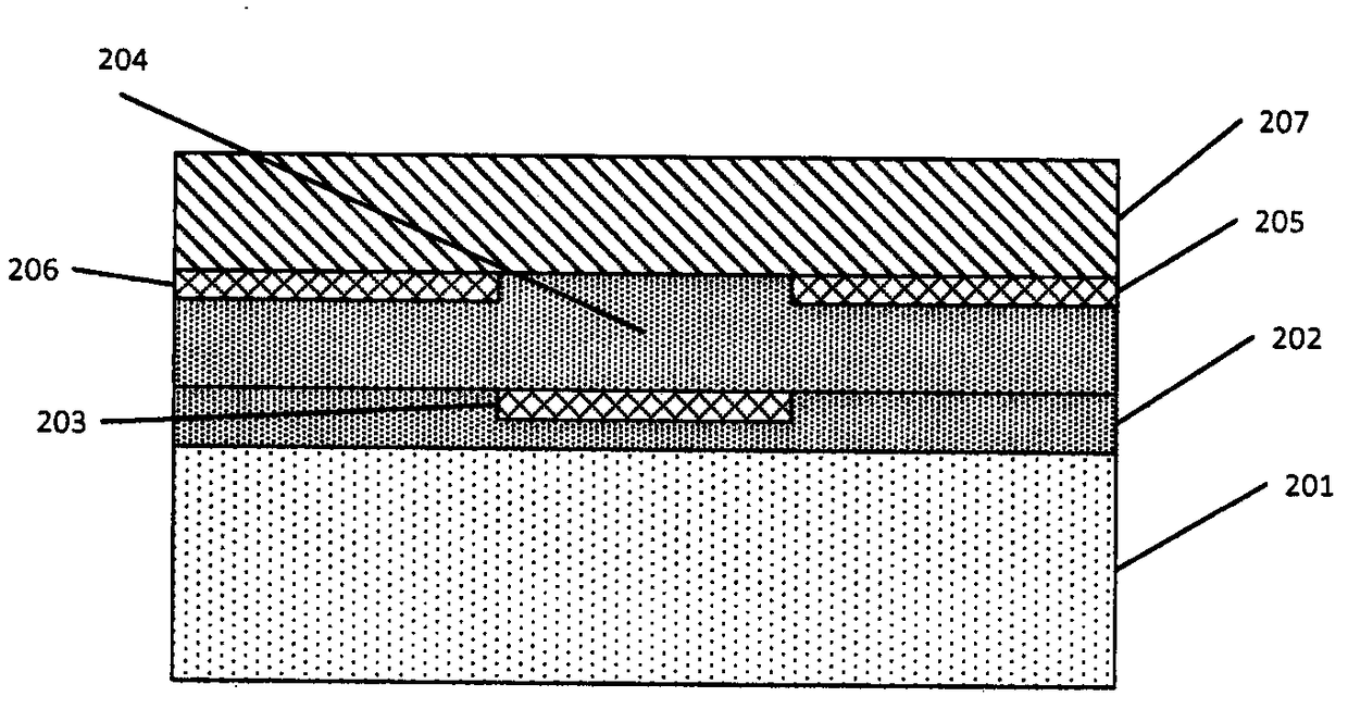
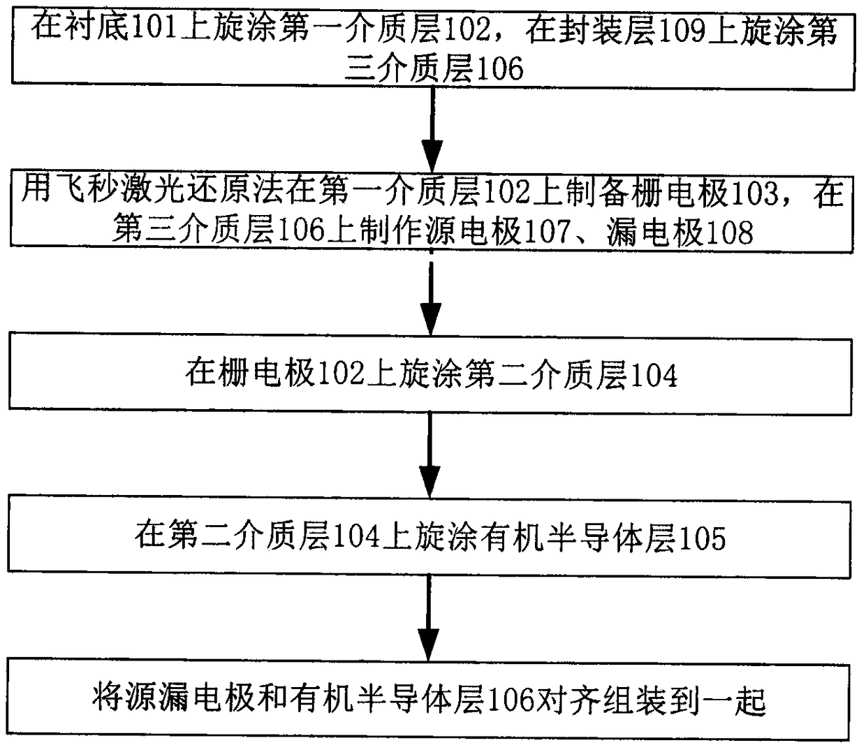
[0048] 1.1 as Figure 6-1 and 6-2 , select PI with a thickness of 90 μm, scrub the PI with detergent powder and cut it into 2cm×2.5cm, and then ultrasonically clean it with acetone, ethanol, and deionized water for 10 minutes respectively.

[0049] 1.2 After the nitrogen gas is blown dry, the surface of the PI is treated with oxygen plasma to make the surface hydrophilic, and the preparation of the substrate 101 and the encapsulation layer 109 is completed.

[0050] step 2

[0051] 2.1 Weigh 30mg of purified graphene oxide powder with an electronic scale, weigh 60ml of ethanol with a measuring cyl...


PUM

PropertyMeasurementUnit
thicknessaaaaaaaaaa
lengthaaaaaaaaaa
thicknessaaaaaaaaaa

Abstract

The present invention proposes an all-graphene group organic field effect tube and a preparation method thereof, and uses the stability and high mobility of the graphene group material to improve the electrical performance of the field effect tube, and at the same time, the graphene group semiconductor material can obtain high High-quality thin films reduce the requirements for equipment in production. At the same time, using graphene oxide femtosecond laser reduction technology can directly form electrodes on the dielectric layer. Automatic production can be realized through software control, which is convenient for large-scale preparation and low production cost. The all-graphene organic field effect transistor of the present invention has two structures, which are respectively a bottom gate top contact organic field effect transistor and a bottom gate bottom contact organic field effect transistor. The difference is that the positions of the source electrode and the drain electrode are different. . The invention can be applied to the manufacture of flexible circuits, such as flexible display screens, smart wearable devices, biosensors, etc., and provides a solution for the further application of organic integrated circuits in the future.

Description

technical field [0001] The invention relates to the field of semiconductor devices, in particular to an all-graphene family flexible organic field effect transistor and a manufacturing method thereof. Background technique [0002] As the most basic electronic component in integrated circuits, field effect transistors are necessary components for the manufacture of various integrated circuits, and are widely used in various electronic products, such as computer chips, mobile phones, digital cameras, etc. Its performance also affects the overall performance of the circuit. Taking computer chips as an example, with the development of integrated circuits, the integration level is getting higher and higher. The current mainstream integration level is 64M, that is, the number of electronic components contained on a single chip. The number is 60 million, and the line width of the most advanced integrated circuit in the world has been reduced to 0.13 microns, that is, the minimum ch...

Claims


Application Information

Patent Timeline
Patent Type & Authority Patents(China)
IPC IPC(8): H01L51/05H01L51/10H01L51/40C01B32/182
CPCH10K10/46H10K10/82H10K77/111Y02E10/549
Inventor 唐莹马力超韦一彭应全王颖
Owner CHINA JILIANG UNIV
Why Eureka
Try Eureka