Gallium Nitride Semiconductor Light-Emitting Diode with Tilted Quantum Barrier Structure and Its Manufacturing Method

A light-emitting diode and multi-quantum well structure technology, which is applied in semiconductor devices, electrical components, circuits, etc., can solve the problems of light-emitting diode efficiency decline, reduce polarization effects, and reduce hole migration barriers, etc., to achieve suppression of recombination efficiency The decline, the solution efficiency decline, the effect of reducing the potential barrier

Active Publication Date: 2017-12-19
杭州增益光电科技有限公司
View PDF7 Cites 0 Cited by
  • Summary
  • Abstract
  • Description
  • Claims
  • Application Information

AI Technical Summary

Problems solved by technology

[0005] In view of the deficiencies in the prior art, the object of the present invention is to provide a gallium nitride semiconductor light-emitting diode with a tilted quantum barrier structure, which reduces the polarization effect and the potential barrier for hole migration through the optimization of the multi-quantum well structure , so that electrons and holes are more evenly distributed in multiple quantum wells, reducing the leakage of electrons, thereby suppressing the decline in recombination efficiency under high current density injection, and solving the problem of efficiency decline in light-emitting diodes

Method used


Image

  • Gallium Nitride Semiconductor Light-Emitting Diode with Tilted Quantum Barrier Structure and Its Manufacturing Method
  • Gallium Nitride Semiconductor Light-Emitting Diode with Tilted Quantum Barrier Structure and Its Manufacturing Method
  • Gallium Nitride Semiconductor Light-Emitting Diode with Tilted Quantum Barrier Structure and Its Manufacturing Method

Examples


Embodiment Construction

[0025] In order to make the object, technical solution and advantages of the present invention clearer, the specific implementation manners of the present invention will be described in detail below in conjunction with the accompanying drawings. Examples of these preferred embodiments are illustrated in the accompanying drawings. The embodiments of the invention shown in and described with reference to the drawings are merely exemplary, and the invention is not limited to these embodiments.

[0026] Here, it should also be noted that, in order to avoid obscuring the present invention due to unnecessary details, only the structures and / or processing steps closely related to the solution according to the present invention are shown in the drawings, and the related Other details are not relevant to the invention.

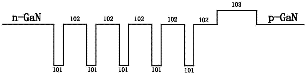
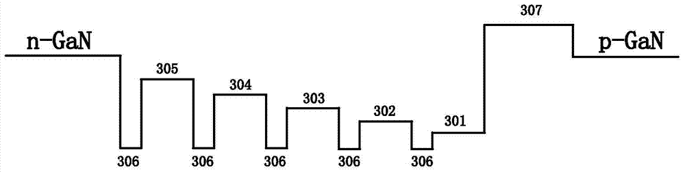
[0027] As mentioned above, in view of the defects of the existing gallium nitride semiconductor light-emitting diodes, the inventors of this case have been able to pr...


PUM


Abstract

The invention discloses a gallium nitride semiconductor light-emitting diode with an inclined quantum barrier structure and a manufacturing method thereof. The light emitting diode comprises an N-type gallium nitride layer, a multi-quantum well structure layer and a P-type gallium nitride layer stacked in sequence, and the multi-quantum well structure layer includes a plurality of indium gallium nitride well layers and a plurality of indium gallium nitride barriers stacked alternately layer, and the molar content of indium in each indium gallium nitride barrier layer gradually decreases along the direction from the p-type gallium nitride layer to the n-type gallium nitride layer. The light emitting diode can be grown and formed by epitaxial process such as MOCVD. With the technical solution of the present invention, not only can the polarization electric field generated by the polarization effect in the quantum well be reduced, but also the recombination efficiency of electron holes in the quantum well can be increased, the potential barrier of hole migration can be reduced, and the electrons and holes can be more uniform. Distributed in multiple quantum wells, it can also effectively reduce the leakage of electrons, thereby improving the luminous efficiency of light-emitting diodes at high current densities, and solving the problem of reduced efficiency in light-emitting diodes.

Description

technical field [0001] The invention relates to a light-emitting diode, in particular to a gallium nitride semiconductor light-emitting diode with an inclined quantum barrier structure, and belongs to the field of gallium nitride semiconductor device design and epitaxial growth. Background technique [0002] In gallium nitride-based light-emitting diodes, due to the large effective mass of holes, the carriers are not uniformly distributed in the multiple quantum wells. Usually, the luminescence of multiple quantum wells mainly comes from 1-2 quantum wells close to the P-type layer. When the injected current density is high, the efficiency of light-emitting diodes will drop. There is also a polarization potential field in the light-emitting diode quantum well grown on the C surface, which makes the conduction band and valence band tilt in the well, and electrons and holes are separated in space, reducing the efficiency of radiative recombination in the well. [0003] Specif...

Claims


Application Information

Patent Timeline
Patent Type & Authority Patents(China)
IPC IPC(8): H01L33/00H01L33/06
Inventor 周坤池田昌夫刘建平张书明李德尧张立群杨辉
Owner 杭州增益光电科技有限公司
Why Eureka
Try Eureka