


Quick Research
Generate reliable direction feasibility study reports for your R&D in just a few steps.

Technical Q&A
Discover and master advanced knowledge NOW. Basics, ideas, possibilities, all at once.

Find Solutions
As an expert in R&D theories, this can generate solutions to your technical problems instantly.

Evaluate Feasibility
Analyze your overall solution with one click, know your potential R&D risks in advance.

Monitor Landscape
Get weekly tech updates, stay abreast of the latest tech innovations and key insights.
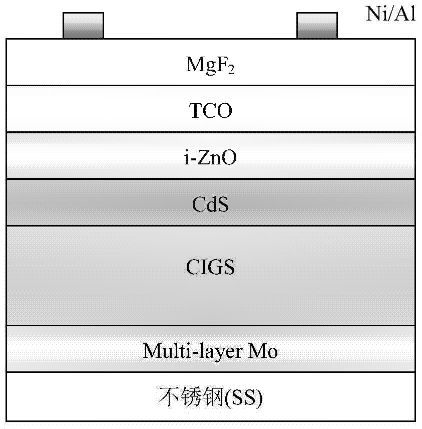
A back electrode structure of flexible cigs thin film solar cells
A technology of thin-film solar cells and thin-film structures, applied in circuits, photovoltaic power generation, electrical components, etc., can solve problems such as adding barrier layers, failure, and film removal, so as to reduce process links, overcome poor bonding force, and improve film-forming quality Effect
- Summary
- Abstract
- Description
- Claims
- Application Information
AI Technical Summary
Problems solved by technology
Method used
Image

Examples
Embodiment 1
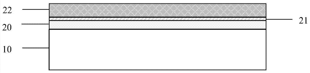
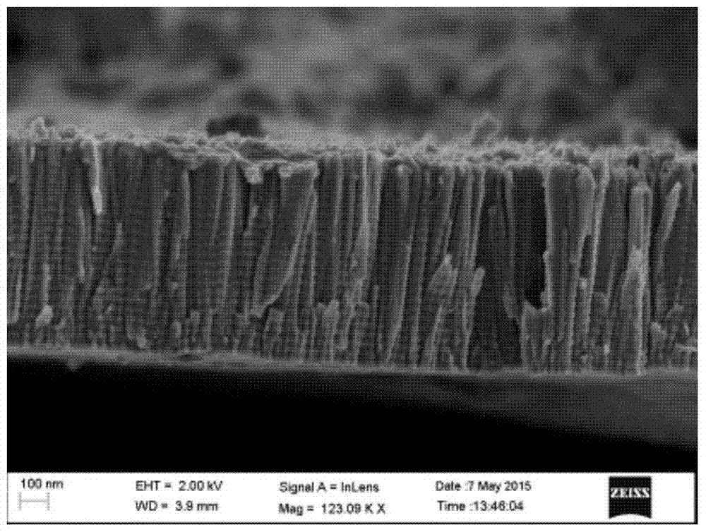
[0022] Such as figure 2 Shown is a schematic diagram of the structure of the back electrode of the flexible CIGS solar cell of the present invention. After the flexible stainless steel substrate 10 is cleaned, put it into a magnetron sputtering machine, the substrate is not heated, and the background vacuum reaches 3×10 -3 When it is below Pa, feed high-purity argon, adjust the air pressure to 1Pa, and the power density to 2.5W / cm 2 , on the flexible stainless steel substrate 10, a layer of 0.12 μm thick Mo film layer 20 is sputtered; after the first layer of Mo is completed, the air pressure is adjusted to 0.8Pa, and the power density is 3W / cm 2 , sputtering a layer of Mo film layer 21 with a thickness of 0.08 μm; after completing the second layer of Mo, adjust the air pressure to 0.3Pa, and the power density to 3.5W / cm 2 , sputtering a layer of 0.6 μm thick Mo film layer 22; the total thickness of the Mo layer is about 0.8 μm, and the resistivity is 3.8×10 -5 Ω·cm, its c...
Embodiment 2
[0024] After cleaning the flexible copper foil substrate, put it into the magnetron sputtering machine, and wait for the local vacuum to reach 3×10 -3 When it is below Pa, feed high-purity argon, adjust the air pressure to 0.3Pa, and the power density to 2.5W / cm 2 , on the flexible copper foil substrate 10, start sputtering a layer of 0.12 μm thick molybdenum film layer; after the first layer of Mo is completed, adjust the air pressure to 0.8Pa, and the power density to 3W / cm 2 , under this process, a layer of molybdenum film with a thickness of 0.08μm is sputtered; after the second layer of Mo is completed, the air pressure is adjusted to 1.2Pa, and the power density is 3.5W / cm 2 , under this process, a layer of molybdenum film with a thickness of 0.6 μm is sputtered. After the third layer of Mo is completed, the air pressure is adjusted to 1.5Pa and the power density is 4W / cm 2 , under this process, sputtering a layer of molybdenum film with a thickness of 0.2 μm, which is ...
Embodiment 3
[0027] After cleaning the flexible aluminum foil, put it into magnetron sputtering, and wait for the local vacuum to reach 3×10 -3 When it is below Pa, feed high-purity argon, adjust the air pressure to 0.3Pa, and the power density to 2.5W / cm 2 , on the flexible stainless steel substrate 10, start sputtering a layer of 0.12 μm thick molybdenum film layer 20; after the first layer of Mo is completed, adjust the air pressure to 0.8Pa, and the power density to 3W / cm 2 , under this process, a layer of molybdenum film layer 21 with a thickness of 0.08 μm is sputtered; after the second layer of Mo is completed, the air pressure is adjusted to 1.2Pa, and the power density is 3.5W / cm 2 , under this process, a layer of molybdenum thin film 22 with a thickness of 0.6 μm is sputtered. After the third layer of Mo is completed, the air pressure is adjusted to 1.5 Pa, and the power density is 4 W / cm 2 , under this process, a layer of molybdenum film layer 23 with a thickness of 0.2 μm is s...
PUM
| Property | Measurement | Unit |
|---|---|---|
| electrical resistivity | aaaaa | aaaaa |
| thickness | aaaaa | aaaaa |
| thickness | aaaaa | aaaaa |
Abstract
Description
Claims
Application Information
 - R&D Engineer
- R&D Manager
- IP Professional
- Industry Leading Data Capabilities
- Powerful AI technology
- Patent DNA Extraction
Browse by: Latest US Patents, China's latest patents, Technical Efficacy Thesaurus, Application Domain, Technology Topic, Popular Technical Reports.
© 2024 PatSnap. All rights reserved.Legal|Privacy policy|Modern Slavery Act Transparency Statement|Sitemap|About US| Contact US: help@patsnap.com