Array substrate and manufacturing method thereof, display panel and display device

An array substrate and display area technology, which is applied in semiconductor/solid-state device manufacturing, optics, instruments, etc., can solve the problems of poor area display, deflection of liquid crystal molecules, and deviation of orientation grooves, and achieves avoiding poor display, reducing the depth of depression, Reduce the effect of bending

Active Publication Date: 2018-06-05
BOE TECH GRP CO LTD +1
View PDF2 Cites 0 Cited by
  • Summary
  • Abstract
  • Description
  • Claims
  • Application Information

AI Technical Summary

Problems solved by technology

However, the above-mentioned auxiliary alignment pattern with a large depth will bend and deform the bristles on the rubbing cloth during rubbing and alignment, so that the alignment groove formed at this position will be deviated, resulting in the deflection of liquid crystal molecules, resulting in poor display in this area

Method used


Image

  • Array substrate and manufacturing method thereof, display panel and display device
  • Array substrate and manufacturing method thereof, display panel and display device
  • Array substrate and manufacturing method thereof, display panel and display device

Examples


Embodiment Construction

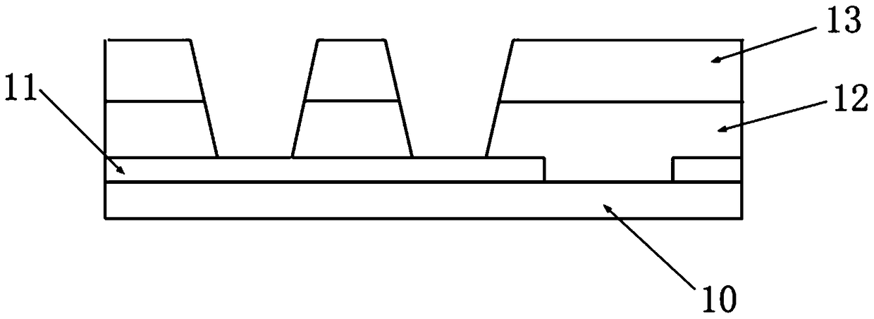
[0038] Specific embodiments of the present invention will be described in detail below in conjunction with the accompanying drawings. It should be understood that the specific embodiments described here are only used to illustrate and explain the present invention, and are not intended to limit the present invention.

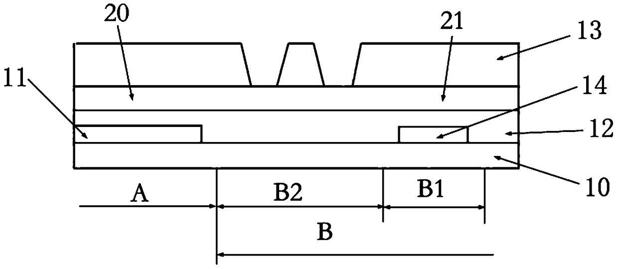
[0039] The present invention provides an embodiment of an array substrate, figure 2 A schematic diagram of an array substrate provided in an embodiment of the present invention. Such as figure 2 As shown, in this embodiment, the array substrate includes a display area A and a non-display area B located around the display area A, and the non-display area B includes a first alignment mark area B1 and an auxiliary alignment mark Area B2; wherein, the auxiliary alignment mark area B2 includes an insulating layer 12, a first etching stopper layer 20 and a passivation layer 13 that are sequentially stacked from bottom to top, and an auxiliary alignment mark is for...


PUM


Abstract

The invention provides an array substrate and a preparation method thereof, a display panel and a display device. The array substrate includes a display area and a non-display area located around the display area, the non-display area includes a first alignment mark area and an auxiliary alignment mark area; the auxiliary alignment mark area includes sequentially from bottom to top An insulating layer, a first etch barrier layer and a passivation layer are stacked, and an auxiliary alignment pattern is formed on the passivation layer; the first alignment mark area includes a first alignment mark that is stacked sequentially from bottom to top , insulating layer and passivation layer. The auxiliary alignment mark region of the above-mentioned array substrate has a first etching barrier layer, which makes the depth of the auxiliary alignment pattern formed by the etching process smaller, so that when the alignment layer is prepared by rubbing alignment, the bristles on the rubbing cloth can be reduced. The bending and deformation can reduce the error of the orientation groove and help to avoid poor display.

Description

technical field [0001] The present invention relates to the field of display technology, in particular, to an array substrate and a preparation method thereof, a display panel and a display device. Background technique [0002] The array substrate includes a display area and a non-display area. figure 1 It is a schematic diagram of the structure of the non-display area of ​​the conventional array substrate. Such as figure 1 As shown, the non-display area of ​​the array substrate includes patterns such as the gate material region 11 , the insulating layer 12 and the passivation layer 13 formed on the base substrate 10 . The above-mentioned gate material region 11 , insulating layer 12 and passivation layer 13 are generally arranged in the same layer as the gate, insulating layer and passivation layer in the display area, and are formed synchronously. Forming these patterns on the base substrate 10 generally requires an exposure process using a mask. [0003] In order to m...

Claims


Application Information

Patent Timeline
Patent Type & Authority Patents(China)
IPC IPC(8): H01L27/12H01L23/544H01L21/77G02F1/1362G02F1/1368
Inventor 蔡振飞慕绍帅彭国昊季雨
Owner BOE TECH GRP CO LTD
Why Eureka
Try Eureka