Method for reducing v-groove on top of polysilicon in trench of trench-type power transistor

A technology for power transistors and polysilicon is applied in the field of reducing the V-shaped groove at the top of polysilicon in the trench of a trench type power transistor, which can solve the problems of increasing the resistance value, the thickness of the ILD, and reducing the window of the Cont etching process, so as to reduce the depression. the effect of depth

Active Publication Date: 2015-08-05
HEJIAN TECH SUZHOU
View PDF8 Cites 0 Cited by
  • Summary
  • Abstract
  • Description
  • Claims
  • Application Information

AI Technical Summary

Problems solved by technology

This V-shaped groove will affect the leakage current of the switching device and increase the resistance of the Cont (contactor) above the gate, thereby affecting the switching speed and power consumption of the switching device. At the same time, the thickness of the ILD (internal dielectric layer) above the gate will increase with the As the depression of the V-shaped groove increases, this situation will narrow the Cont etching process window. When the depression reaches a certain level, it is more likely that the thickness of the ILD will be too thick to be etched cleanly, so that the Cont cannot be well connected to the gate, resulting in Switching device failure
[0004] At present, there are two improved processes that can solve the above problems: the first is to increase the thickness of polysilicon deposition (about 10K), but this process is not effective while increasing the cost; the second is to add a step before polysilicon etching Polysilicon CMP (Chemical Mechanical Polishing, chemical mechanical polishing) process, this process makes the polysilicon in the trench and the polysilicon above the source almost at the same level, and can significantly improve the V-shaped groove during etching, but the cost of polysilicon CMP is relatively high

Method used


Image

  • Method for reducing v-groove on top of polysilicon in trench of trench-type power transistor
  • Method for reducing v-groove on top of polysilicon in trench of trench-type power transistor
  • Method for reducing v-groove on top of polysilicon in trench of trench-type power transistor

Examples


Embodiment Construction

[0025] In order to make the object, technical solution and advantages of the present invention clearer, the present invention will be further described in detail below in conjunction with the accompanying drawings and embodiments. It should be understood that the specific embodiments described here are only used to explain the present invention, not to limit the present invention.

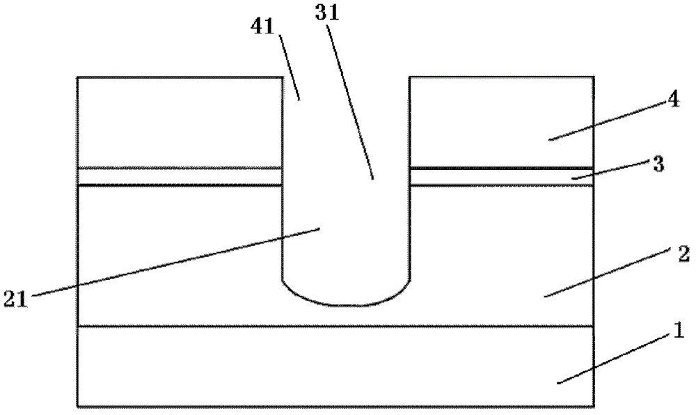
[0026] Such as Figure 1 to Figure 8 As shown, the present invention provides a method for reducing the V-shaped groove at the top of the polysilicon in the groove of the trench power transistor, comprising the following steps:

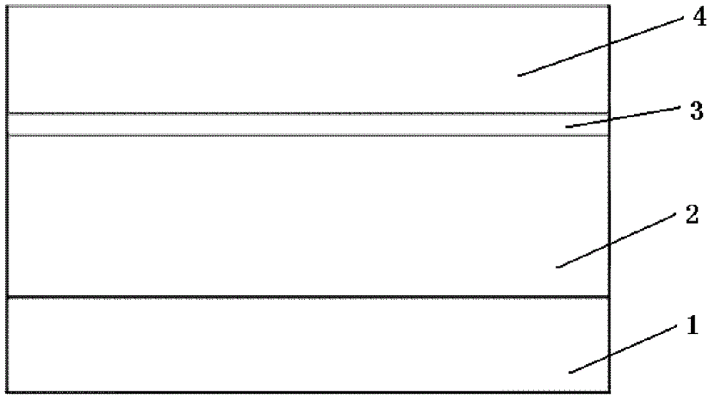
[0027] Step 1: If figure 1 As shown, the present invention provides a substrate 1, an epitaxial layer 2 is provided on the upper surface of the substrate 1, a pad oxide layer 3 is provided on the upper surface of the epitaxial layer 2, and a hard mask layer 4 is provided on the upper surface of the pad oxide layer 3; In this embodiment, the substrate 1 is an N+ substrat...


PUM


Abstract

The invention discloses a method of reducing a V-shaped groove at the top end of polycrystalline silicon inside a groove of a groove-type power transistor. The method comprises a first step of forming the groove on the power transistor, depositing the polycrystalline silicon inside the groove to form a grid and form the V-shaped groove at the top end of the polycrystalline silicon at the same time, depositing the polycrystalline silicon used for filling the V-shaped groove on the upper surface of the grid, and the etched and deposited polycrystalline silicon forming the V-shaped groove with a small depth. The method can greatly reduce the depth of the V-shaped groove at the top end of the polycrystalline silicon, reduce contactor (Cont) resistance on the grid, and prevent a switch component from losing effectiveness because the Cont resistance can not be connected with the grid. The method can be widely applied to forming of the grid inside the groove of the groove-type power transistor.

Description

technical field [0001] The invention relates to the technical field of semiconductors, in particular to a method for reducing the V-shaped groove at the top of polysilicon in the trench of a trench-type power transistor. Background technique [0002] At present, power transistors are widely used in high-power switching devices, and such devices generally adopt a vertical conductive structure. In terms of the physical structure of the device, the trench structure is one of the typical structures, and it is widely used. [0003] The gate of the trench power transistor is located in the trench, and when forming the gate, it is necessary to fill the trench with polysilicon. In conventional processes, polysilicon is deposited to a thickness of approximately 6K. Because the trench is very deep (depth > 1.0 um), after the polysilicon fills the trench, the height of the top surface of the polysilicon in the trench in the horizontal direction is lower than that of the source. A...

Claims


Application Information

Patent Timeline
Patent Type & Authority Patents(China)
IPC IPC(8): H01L21/336H01L21/28
Inventor 石亮孙张虎施晓东瞿学峰
Owner HEJIAN TECH SUZHOU
Why Eureka
Try Eureka