
Method for growing substrate-modified large-size monolayer molybdenum disulfide film through chemical vapor deposition

A technology of chemical vapor deposition and single-layer molybdenum disulfide, which is applied in gaseous chemical plating, coating, metal material coating technology, etc., can solve the problems of small film size and difficult control of film thickness, and achieve long preparation time Effect

Active Publication Date: 2015-10-28
NANJING UNIV
View PDF4 Cites 34 Cited by
  • Summary
  • Abstract
  • Description
  • Claims
  • Application Information

AI Technical Summary

Problems solved by technology

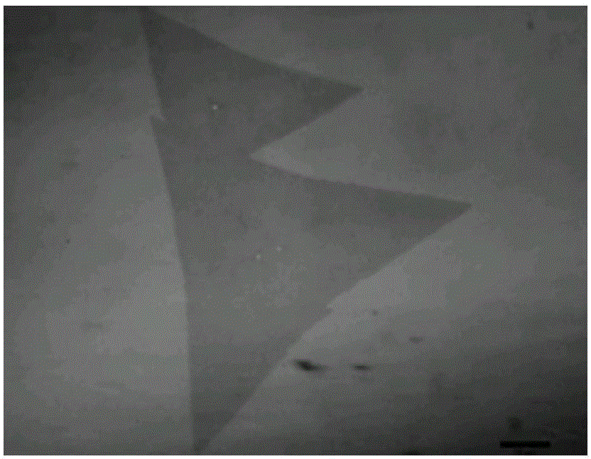
[0005] The purpose of the present invention is to overcome the shortcomings of the current chemical vapor deposition growth molybdenum disulfide film size is small, the film thickness is not easy to control, to propose a method for substrate surface modification chemical vapor deposition growth large-scale monolayer molybdenum disulfide

Method used


Image

  • Method for growing substrate-modified large-size monolayer molybdenum disulfide film through chemical vapor deposition
  • Method for growing substrate-modified large-size monolayer molybdenum disulfide film through chemical vapor deposition
  • Method for growing substrate-modified large-size monolayer molybdenum disulfide film through chemical vapor deposition

Examples


Embodiment 1

[0024] A silicon-silicon dioxide substrate is used as the growth substrate, and the thickness of the silicon dioxide layer heat-treated on the silicon surface is 300 nm. The substrate processing process is as follows: first clean the silicon-silica substrate, ultrasonically clean with acetone, ethanol and deionized water for 10 minutes, and then use a mixed solution of sulfuric acid and hydrogen peroxide with a volume ratio of 3:1 in 160 Clean at ℃ for 30 minutes, and then ultrasonically clean with deionized water for 5 minutes to remove excess concentrated sulfuric acid on the surface; put the cleaned silicon-silica substrate into 40-44wt% ammonia sulfide solution for 24 hours and soak The resulting silicon-silica substrate was finally ultrasonically cleaned in deionized water for 2 minutes, and the substrate was blown dry with high-purity nitrogen; the dried silicon-silica substrate was stored in vacuum for 24 hours to remove residual organic matter. Anneal the above substrat...

Embodiment 2

[0029] With aluminum oxide (Al 2 O 3 ) The substrate is a growth substrate, and the film deposition surface is the (100) surface of aluminum oxide. The substrate processing process is as follows: firstly, the aluminum oxide substrate is cleaned, ultrasonically cleaned with acetone, ethanol and deionized water for 10 minutes, and then a mixed solution of sulfuric acid and hydrogen peroxide in a volume ratio of 3:1 is used at 160℃ After cleaning for 30 minutes, and then ultrasonic cleaning with deionized water for 5 minutes to remove the excess concentrated sulfuric acid on the surface; put the cleaned aluminum oxide substrate into 40-44wt% ammonia sulfide solution for 24 hours, and the Finally, the aluminum oxide substrate was ultrasonically cleaned in deionized water for 2 minutes, and the substrate was blown dry with high-purity nitrogen; the blown-dried aluminum oxide substrate was stored in vacuum for 24 hours to remove residual organic matter. . Anneal the above substrate ...


PUM

PropertyMeasurementUnit
Thicknessaaaaaaaaaa
Sizeaaaaaaaaaa

Abstract

The invention proposes a method for growing a substrate-modified large-size monolayer molybdenum disulfide film through chemical vapor deposition. Ammonium sulfide serves as a substrate surface modifying agent; a nucleation rate is controlled through such methods as control of a concentration of the modifying agent, a dipping time and a cleaning method; and a film thickness is controlled through such methods as control of a growing temperature, a growing time and an air flow of the chemical vapor deposition. The method can efficiently grow the large-size monolayer molybdenum disulfide film under the condition of a relatively lower growing temperature on the basis of traditional growth chemical vapor deposition equipment. The method for growing large-size monolayer molybdenum disulfide, provided by the invention, is suitable for the growth of large-size monolayer tungsten disulfide, molybdenum diselenide, tungsten diselenide and the like similar to two-dimensional semiconductor materials in structure.

Description

Technical field [0001] The invention relates to a method for preparing a thin film by chemical vapor deposition, in particular to a method for growing a large-size single-layer molybdenum disulfide film by chemical vapor deposition with a substrate modification. Background of the invention [0002] Single-layer molybdenum disulfide (MoS2) is a new type of two-dimensional semiconductor material with an ideal energy band gap (1.8eV). The field effect transistor (FET) based on it can not only obtain 10 8 The high switching ratio, and has lower energy loss. On the other hand, the monolayer structure of molybdenum disulfide crystal is a direct band gap semiconductor, and the change of the band structure can effectively improve the fluorescence efficiency and light absorption cross section of the monolayer molybdenum disulfide. In the honeycomb structure of a single layer of molybdenum disulfide, molybdenum atoms and sulfur atoms alternately occupy adjacent lattice sites, and the centr...

Claims


Application Information

Patent Timeline
IPC IPC(8): C23C16/30C23C16/02
Inventor 王迪王牧彭茹雯蒋尚池熊翔姚鹏飞赵地
Owner NANJING UNIV
Learn More