
UV-LED with quantum dot structure

A technology of light-emitting diodes and quantum dots, which is applied in semiconductor devices, electrical components, circuits, etc., can solve the problems of insignificant electron overflow hole injection efficiency and insufficient energy bandgap, so as to enhance luminous power and brightness, eliminate energy With bending, the effect of improving compound efficiency

Active Publication Date: 2015-10-07
江西力特康光学有限公司
View PDF2 Cites 11 Cited by
  • Summary
  • Abstract
  • Description
  • Claims
  • Application Information

AI Technical Summary

Problems solved by technology

However, for AlGaN-based ultraviolet LEDs, since the energy band gap of the above-mentioned EBL layer is not large enough, it will not only absorb the ultraviolet light emitted by the LED itself, but also prevent the overflow of electrons and improve the efficiency of hole injection.

Method used


Image

  • UV-LED with quantum dot structure
  • UV-LED with quantum dot structure

Examples


Embodiment Construction

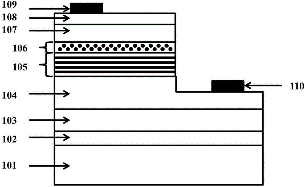
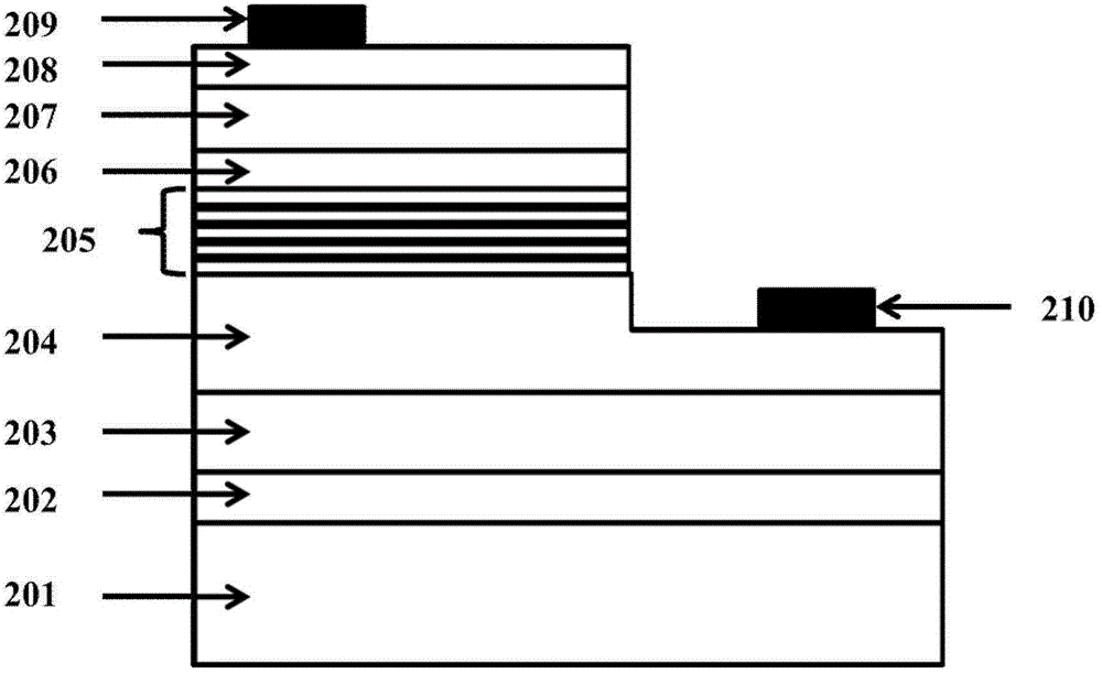
[0017] Such as figure 1 As shown, a UV-LED with a p-type AlN / AlGaN quantum dot electron blocking layer structure includes a sapphire substrate 101, an AlN nucleation layer 102, an undoped AlGaN buffer layer 103, and an n-type AlGaN layer 104, Al x Ga 1-x N / Al y Ga 1-y N multi-quantum well active region 105, p-type AlN / AlGaN quantum dot electron blocking layer 106, p-type AlGaN layer 107 and indium tin oxide conductive layer (ITO) 108, n-type ohmic electrode 110 drawn on the n-type AlGaN layer , a p-type ohmic electrode 109 drawn on an indium tin oxide conductive layer (ITO).

[0018] Preferably, the sapphire substrate 101 is an r-plane sapphire substrate.

[0019] Preferably, the thickness of the AlN nucleation layer 102 is 20-100nm, the thickness of the non-doped AlGaN buffer layer 103 is 100-800nm, the thickness of the n-type AlGaN layer 104 is 800-1000nm, Al x Ga 1-x N / Al y Ga 1-y The period number of the N multi-quantum well active region 105 is 5-10, the thickne...


PUM


Abstract

The invention discloses an UV-LED with a quantum dot EBL, comprising a sapphire substrate, an A1N nucleating layer, a non-doped u type A1GaN buffer layer, an n type A1GaN layer, an A1xGa1-xN / A1yGa1-yN quantum well active region, a p type A1N / A1GaN quantum dot EBL, a p type A1GaN layer and an ITO conductive layer. An n type ohmic electrode is lead out on the n type A1GaN layer, and a p type ohmic electrode is lead out on the ITO conductive layer. The UV-LED with a quantum dot EBL employs the p type doping layer of self-assembly A1N / A1GaN quantum dots as the EBL and a hole injection layer, which can effectively inhibit electrons from overflowing out of an active region, enhance the efficiency of hole injection to the active region, and thereby increase the carrier composite efficiency in the active region; in addition, A1N is used as the EBL to replace the A1GaN commonly used in blue LED, which can more effectively reduce UV absorption by the EBL, and increase UV-LED luminous efficiency.

Description

technical field [0001] The invention relates to the field of manufacturing semiconductor optoelectronic devices, in particular to an ultraviolet light emitting diode (UV-LED) with a quantum dot electron blocking layer (EBL) structure. Background technique [0002] The ultraviolet spectrum includes all light with wavelengths from 100 to 400nm and is generally subdivided into three categories: long-wave ultraviolet (315-400nm, UV-A), medium-wave ultraviolet (280-315nm, UV-B) and short-wave ultraviolet (100- 280nm, UV-C). Compared with the visible band, ultraviolet photons have higher energy, stronger penetrating ability, and powerful lethality to living things. Due to these properties, ultraviolet light sources have great application value in the fields of high color rendering index solid-state lighting, biochemical harmful substance detection, water purification, high-density storage, and short-wavelength safe communication. In addition, the use of solar-blind ultraviolet l...

Claims


Application Information

Patent Timeline
Patent Type & Authority Applications(China)
IPC IPC(8): H01L33/06H01L33/14H01L33/16
CPCH01L33/06H01L33/145H01L33/16H01L33/32
Inventor 张雄栾华凯崔一平
Owner 江西力特康光学有限公司
Learn More