Method for direct and rapid preparation of single-layer graphene on SiO2/Si substrate
A single-layer graphene and substrate technology, applied in the field of direct and rapid preparation of single-layer graphene on SiO2/Si substrate, can solve problems such as high background vacuum, and achieve the effect of simplifying synthesis and simple and fast preparation process
- Summary
- Abstract
- Description
- Claims
- Application Information
AI Technical Summary
Problems solved by technology
Method used
Image
Examples
Embodiment 1
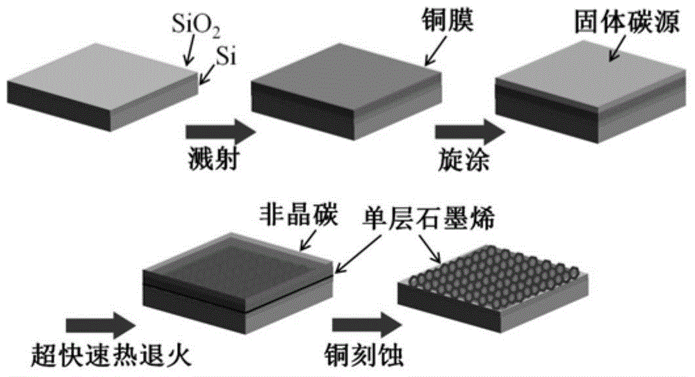
[0027] This embodiment is used to illustrate the present invention in SiO 2 A simple heat treatment method for direct and rapid synthesis of large-area and high-quality single-layer graphene on Si substrates using solid-state carbon sources. Such as figure 1 As shown, the specific steps of the method are as follows:
[0028] 1. On SiO 2 / Si substrate deposited a layer of crystallized copper film
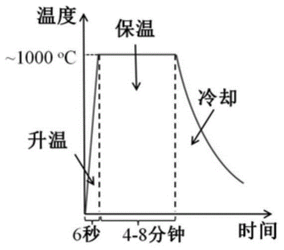
[0029] Surface covered with 300nm SiO 2 layer of silicon as the substrate, using the magnetron sputtering method on SiO 2 A copper film with a thickness of 500nm was deposited on the / Si substrate, and the reference pressure of the sputtering chamber was about 2×10 -6 Torr, the copper deposition rate is controlled at less than Copper-deposited SiO 2 / Si substrate is placed in a common thermal annealing furnace for thermal annealing to crystallize the copper film; during the entire annealing process, the annealing furnace is fed with protective gas Ar / H 2 (1:1); the annealing ...
Embodiment 2
[0038] This embodiment is used to illustrate the present invention in SiO 2 A facile thermal treatment method for the direct and rapid synthesis of single-layer graphene on Si substrates using solid-state carbon sources.
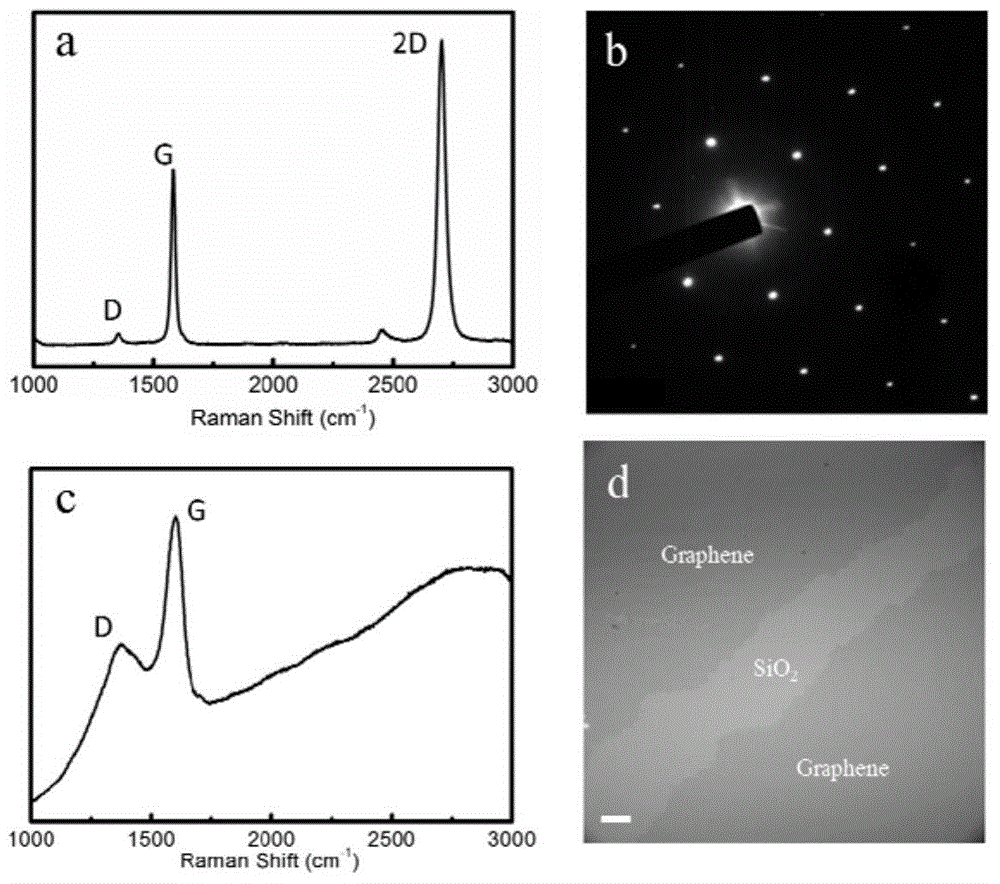
[0039] According to the method identical with embodiment 1 in SiO 2 / Si substrate directly synthesized graphene, the difference is the use of sucrose (Sucrose,C 12 h 22 o 11 ) is the carbon source. After diluting sucrose with ultrapure water, it was spin-coated on the surface of the copper film, and the spin-coating thickness was about 500 nm. Using Raman spectroscopy (such as Figure 5 The bottommost curve in ) confirms that in SiO 2 / Si substrates obtained high-quality single-layer graphene.
PUM
| Property | Measurement | Unit |
|---|---|---|
| thickness | aaaaa | aaaaa |
| thickness | aaaaa | aaaaa |
Abstract
Description
Claims
Application Information
 - R&D
- Intellectual Property
- Life Sciences
- Materials
- Tech Scout
- Unparalleled Data Quality
- Higher Quality Content
- 60% Fewer Hallucinations
Browse by: Latest US Patents, China's latest patents, Technical Efficacy Thesaurus, Application Domain, Technology Topic, Popular Technical Reports.
© 2025 PatSnap. All rights reserved.Legal|Privacy policy|Modern Slavery Act Transparency Statement|Sitemap|About US| Contact US: help@patsnap.com


