A kind of conductive film, the preparation method of conductive film and the ink used therefor
A conductive film and ink technology, which is applied in the field of conductive film, ink, and conductive film preparation, can solve the problems of poor conductivity of conductive film, low conductivity of carbon materials, and inferior metal fillers, etc., and achieve the effect of low cost
- Summary
- Abstract
- Description
- Claims
- Application Information
AI Technical Summary
Problems solved by technology
Method used
Image

Examples
preparation example Construction
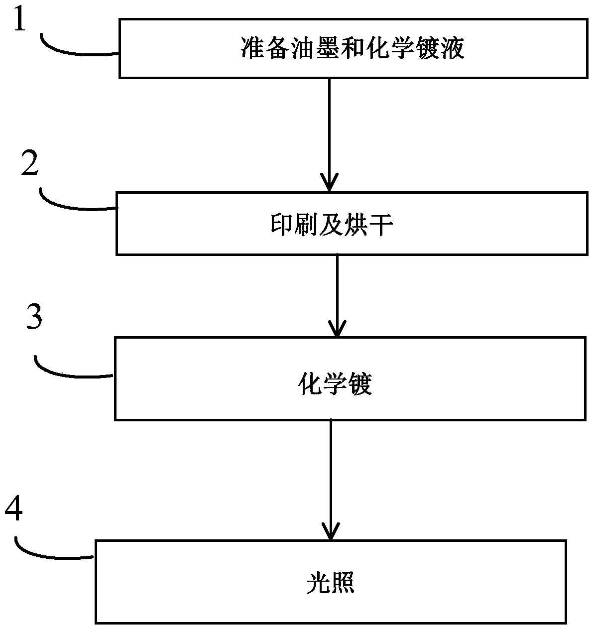
[0017] Such as figure 1 Shown, be the preparation method of the conductive film of this specific embodiment, comprise the following steps:
[0018] 1) Prepare ink and electroless plating solution, wherein the ink includes a main component, an additive and a solvent, and the main component is composed of a photocurable resin with a mass fraction of 10% to 60% and a metal filler with a mass fraction of 40% to 90% , the metal in the filler is more active than the target metal, and the electroless plating solution is a plating solution corresponding to the target metal ion; wherein, the target metal is the type of metal in the conductive film to be prepared.
[0019] Here, the target metal is the kind of metal that plays a conductive role in the conductive film to be finally formed. For example, to make a copper conductive film, then copper is the target metal, and the electroless plating solution is an electroless copper plating solution; to make a nickel conductive film, then n...
experiment example 1
[0035] In this experimental example, epoxy acrylate free radical photocurable resin was used as a binder, and 50 nanometer zinc powder was used as a filler to prepare a main component with a zinc content of 60%, and then mixed with additives and solvents to prepare an ink. The main component of the electroless plating solution is copper sulfate, with a small amount of stabilizer and buffer added. The selected lighting equipment has two lamp heads, one is an ultraviolet lamp tube with a power of 50w, and the other is a xenon flash tube with a single pulse energy of 200J, a pulse width of 2 milliseconds, and a frequency of 10Hz. The irradiation area of the two lamp heads is the same.
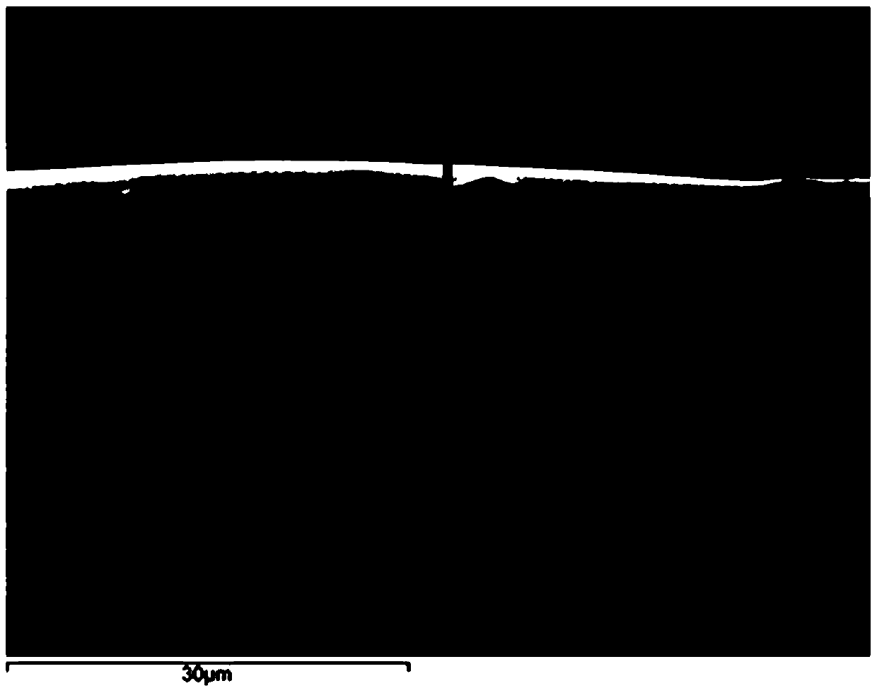
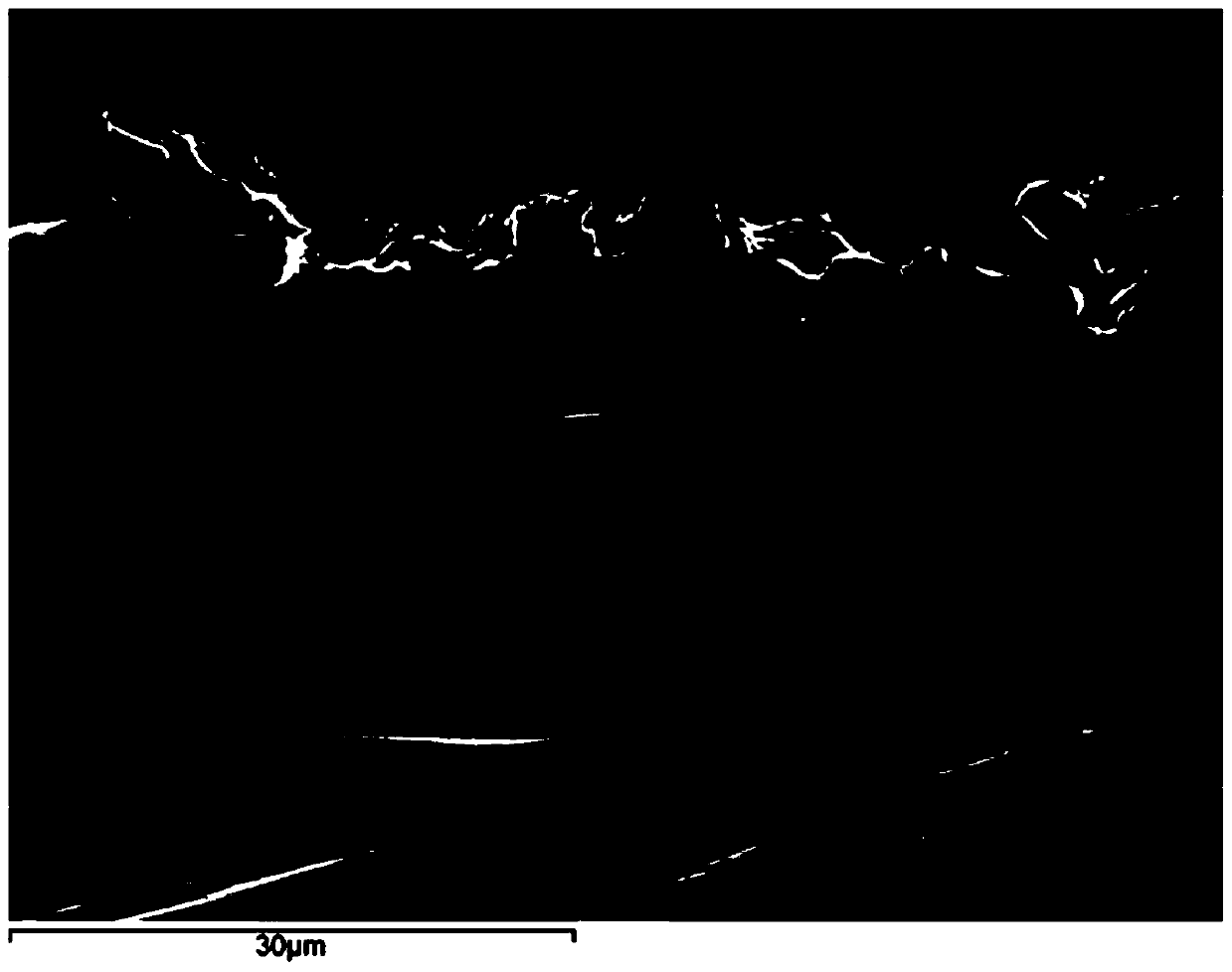
[0036] Printed by screen printing technology, the substrate is PET. A patterned circuit was printed on a PET substrate by screen printing, and then baked at 80° C. for 30 minutes to obtain a circuit pattern formed by a prepreg film. Such as figure 2 Shown is the SEM image of the cross-section...
experiment example 2
[0048] The difference between this experimental example and experimental example 1 is that this experimental example adopts a lithography process, while the experimental example 1 adopts a screen printing process.
[0049] In this experimental example, a cationic epoxy compound photocurable resin was used as a binder and 500 nanometer zinc powder was used as a filler to prepare a main component with a zinc content of 65%, and then mixed with additives and solvents to prepare an ink. The types and amounts of solvents and additives make the ink suitable for lithographic printing. The main component of the electroless plating solution is copper sulfate, with a small amount of stabilizer and buffer added. The selected lighting equipment has two lamp heads, one is an ultraviolet lamp tube with a power of 50w, and the other is a xenon flash tube with a single pulse energy of 200J, a pulse length of 5 milliseconds, and a frequency of 10Hz. The irradiation area of the two lamp heads...
PUM
| Property | Measurement | Unit |
|---|---|---|
| particle diameter | aaaaa | aaaaa |
Abstract
Description
Claims
Application Information
 - R&D
- Intellectual Property
- Life Sciences
- Materials
- Tech Scout
- Unparalleled Data Quality
- Higher Quality Content
- 60% Fewer Hallucinations
Browse by: Latest US Patents, China's latest patents, Technical Efficacy Thesaurus, Application Domain, Technology Topic, Popular Technical Reports.
© 2025 PatSnap. All rights reserved.Legal|Privacy policy|Modern Slavery Act Transparency Statement|Sitemap|About US| Contact US: help@patsnap.com