Sheet-like tungsten trioxide photoelectrode and preparation method thereof
A photoelectrode and sheet-like technology, applied in the direction of electrodes, electrolytic processes, electrolytic components, etc., can solve the problems of poor bonding between the film and the substrate, high film compactness, and small specific surface area, and achieve controllable morphology and low production costs. Low, repeatable effect
- Summary
- Abstract
- Description
- Claims
- Application Information
AI Technical Summary
Problems solved by technology
Method used
Image
Examples
Embodiment 1
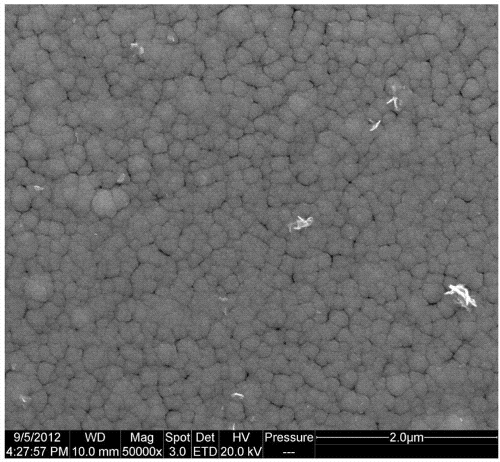
[0038] (1) Place a clean FTO conductive glass substrate 170mm above the sputtering target, and control the background vacuum to be less than 7×10 -7 torr, the substrate is not heated. Using DC reactive sputtering, adjust the sputtering process parameters: working pressure is 10mtorr, reaction gas O 2 The air pressure is 2mtorr, sputtering 50nm tungsten oxide first, and then co-sputtering, the Al target sputtering power is 60W, the W target sputtering power is 150W, the pre-sputtering is 15 minutes, and the sputtering time is 1 hour, and the thickness is about 800nm Al-W-O dense film, the morphology is as follows figure 1 shown.
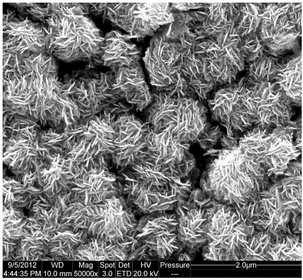
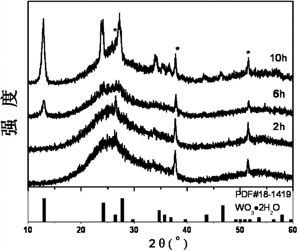
[0039] (2) The obtained mixed-phase amorphous oxide film was exposed to 1M H 2 SO 4 Soaked in the solution for 10 hours, the appearance is as figure 2 shown. The flaky tungsten oxide thin film prepared in this embodiment is evenly distributed, with a thickness of about 30 nm and a size of 220 nm. And from image 3 It can be seen from the XR...
Embodiment 2
[0043] (1) Place a clean FTO conductive glass substrate 170mm above the sputtering target, and control the background vacuum to be less than 7×10 -7 torr, the substrate is not heated. Using DC reactive sputtering, adjust the sputtering process parameters: working pressure is 7.5mtorr, reaction gas O 2 The pressure is 2mtorr, first sputtering 30nm thick tungsten oxide, and then co-sputtering, the Cu target sputtering power is 80W, the W target sputtering power is 200W, the pre-sputtering is 15 minutes, and the sputtering time is 1 hour, and the thickness is about Cu-W-O dense film of 1000nm.
[0044] (2) The obtained mixed-phase amorphous oxide film was exposed to 1M H 2 SO 4 Etched in solution for 8 hours, Figure 8 It is a scanning electron microscope picture, the sheet thickness is about 45nm, and the size is about 670nm.
Embodiment 3
[0046] (1) Place a clean FTO conductive glass substrate above the sputtering target, and control the background vacuum to be less than 7×10 -7 torr, the substrate is not heated. Using DC reactive sputtering, adjust the sputtering process parameters: working pressure is 10mtorr, reaction gas O 2 The air pressure is 2mtorr, first sputtering 50nm thick tungsten oxide, and then co-sputtering, the distance between the W target and the substrate is kept at 150mm, the distance between the Zn target and the substrate is 170mm, the sputtering power of the Zn target is 60W, and the sputtering power of the W target is 150W , pre-sputtering for 15 minutes, and sputtering time for 1 hour, a dense Zn-W-O thin film with a thickness of about 710 nm was obtained.
[0047] (2) The obtained mixed-phase amorphous oxide film was exposed to 1M H 2 SO 4 Etched in solution for 4 hours, Figure 9 It is a scanning electron microscope picture, the sheet thickness is about 45nm, and the size is about...
PUM
| Property | Measurement | Unit |
|---|---|---|
| Thickness | aaaaa | aaaaa |
| Thickness | aaaaa | aaaaa |
| Thickness | aaaaa | aaaaa |
Abstract
Description
Claims
Application Information
 - R&D
- Intellectual Property
- Life Sciences
- Materials
- Tech Scout
- Unparalleled Data Quality
- Higher Quality Content
- 60% Fewer Hallucinations
Browse by: Latest US Patents, China's latest patents, Technical Efficacy Thesaurus, Application Domain, Technology Topic, Popular Technical Reports.
© 2025 PatSnap. All rights reserved.Legal|Privacy policy|Modern Slavery Act Transparency Statement|Sitemap|About US| Contact US: help@patsnap.com


