Vertical structure algan/gan HEMT device and fabrication method thereof

A vertical structure and device technology, applied in semiconductor/solid-state device manufacturing, semiconductor devices, electrical components, etc., can solve problems such as large leakage, lattice damage, and complexity, and achieve low resistivity, enhanced withstand voltage characteristics, and withstand voltage The effect of property changes

Active Publication Date: 2018-02-02
SUZHOU NENGWU ELECTRONICS TECH
View PDF5 Cites 0 Cited by
  • Summary
  • Abstract
  • Description
  • Claims
  • Application Information

AI Technical Summary

Problems solved by technology

[0007] However, regardless of the use of Mg ion implantation or doping, on the one hand, it will introduce lattice damage, especially for the current blocking layer, resulting in a large leakage. On the other hand, Mg has a strong memory effect, which has a great impact on the secondary epitaxy Diffusion
The leakage and current collapse effects caused by the lattice damage caused by Al ion implantation are particularly serious. The reason for this current collapse is mainly due to the defects introduced by Al implantation, and the lattice damage caused by Al implantation must be performed at a very high temperature. It can only be repaired, and the temperature is about 1350°C. It is more complicated and relatively expensive for industrial use. At the same time, the lattice damage caused by large-scale ion implantation has an impact on the crystal quality of the secondary epitaxy.
These problems have always been the bottleneck restricting the development of vertical structure HEMT devices

Method used


Image

  • Vertical structure algan/gan HEMT device and fabrication method thereof
  • Vertical structure algan/gan HEMT device and fabrication method thereof
  • Vertical structure algan/gan HEMT device and fabrication method thereof

Examples


Embodiment Construction

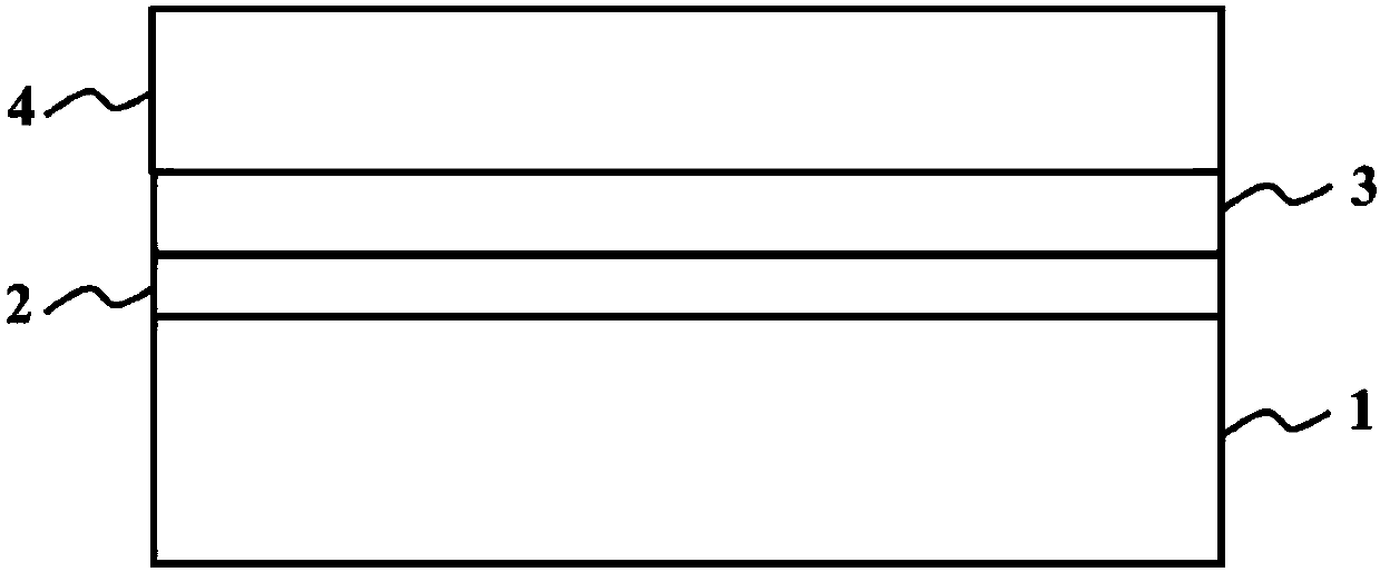
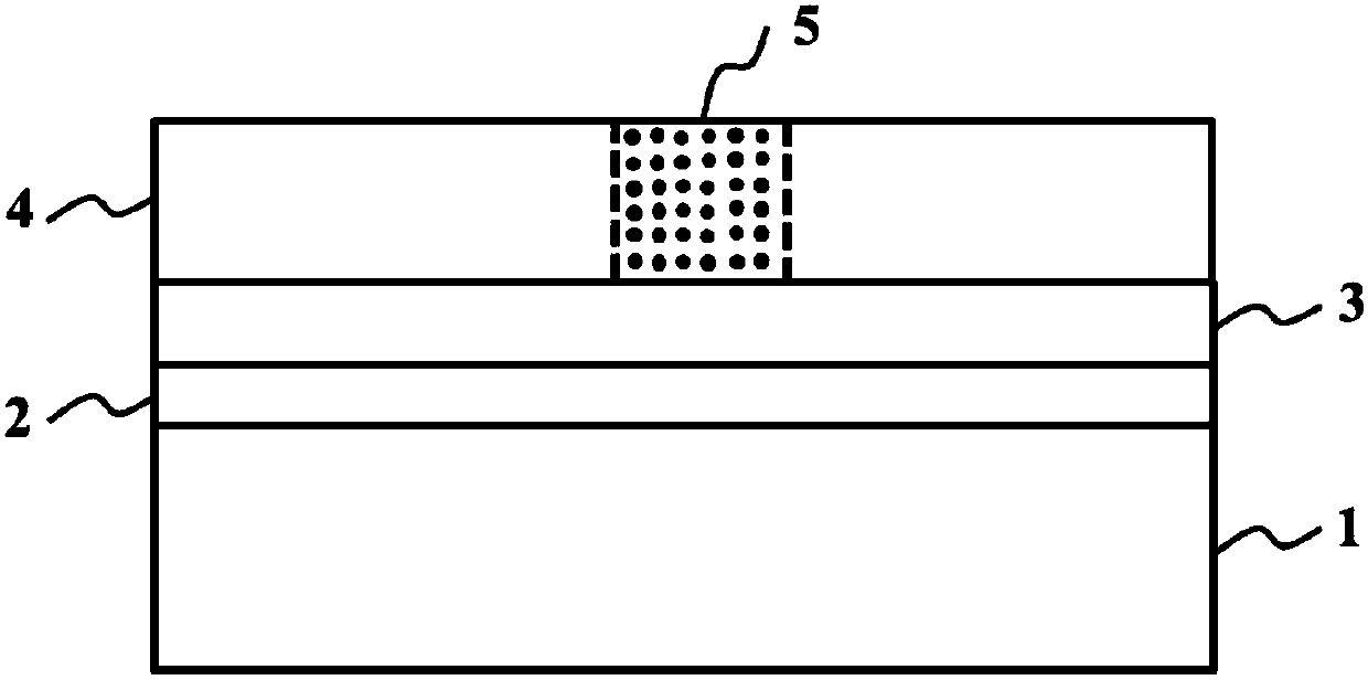
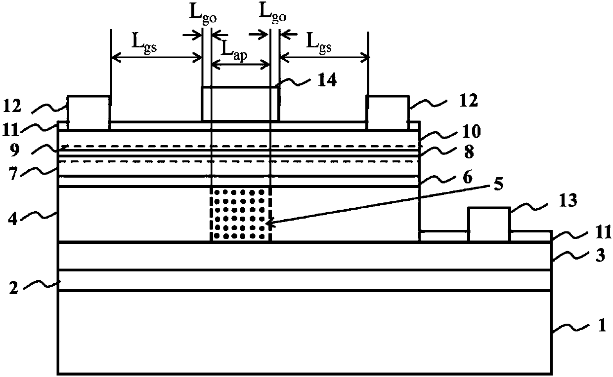
[0031] The embodiment of the present invention discloses a vertical structure AlGaN / GaN HEMT device, including a substrate, and an n+GaN layer, a high-resistance GaN layer, an intrinsic GaN layer, and an AlGaN layer sequentially formed on the substrate, and also includes A drain electrode forming ohmic contact with the n+GaN layer, a source electrode forming ohmic contact with the AlGaN layer, and a gate electrode, the high-resistance GaN layer serving as a current blocking layer including a current formed by Si ion implantation The through hole is conducted, and the current conduction through hole penetrates the high-resistance GaN layer up and down.

[0032]In the above-mentioned vertical structure AlGaN / GaN HEMT device, n+GaN and high-resistance GaN are epitaxially grown for the first time by MOCVD, and the intrinsic GaN layer and the AlGaN layer are formed by secondary epitaxy by MOCVD.

[0033] In this technical scheme, the existing high-resistance GaN is used as the curr...


PUM


Abstract

The invention discloses a vertical structure AlGaN / GaN HEMT device, comprising a substrate, and an n+GaN layer, a high-resistance GaN layer, an intrinsic GaN layer and an AlGaN layer sequentially formed on the substrate, and the n The GaN layer forms a drain electrode in ohmic contact, a source electrode in ohmic contact with the AlGaN layer, and a gate electrode; the high-resistance GaN layer is used as a current blocking layer, which includes a current conduction formed by Si ion implantation holes, and the current conduction via holes penetrate the high-resistance GaN layer up and down. The invention also discloses a manufacturing method of the vertical structure AlGaN / GaN HEMT device. The present invention can realize the vertical structure on relatively low-cost sapphire (sapphire) or Si substrate, and also has the advantages of good current blocking, current transmission, high withstand voltage, low leakage and the like.

Description

technical field [0001] The invention relates to a semiconductor device, in particular to a vertical structure AlGaN / GaN HEMT device and a method for conducting a channel for current transmission. Background technique [0002] In 1993, Khan et al. produced the first GaN-based metal-semiconductor field-effect transistor (MESFET) AlGaN / GaN high electron mobility transistor (HEMT), see Appl.Phys.Lett, 1993, Vol.63(9): 1214- 1215. Although the performance, energy consumption, and figure of merit of the horizontal structure AlGaN / GaN are better than Si devices, there are still some problems that restrict the commercialization of GaN devices, such as AlGaN / GaN HFET under large gate bias or high frequency conditions There will be a current collapse effect, the "self-heating effect" that will occur when the AlGaN / GaN HFET works in a high-temperature, high-power environment, which will reduce the microwave power characteristics of the device, and the problem that it is not easy to be...

Claims


Application Information

Patent Timeline
Patent Type & Authority Patents(China)
IPC IPC(8): H01L29/36H01L29/778H01L21/335
Inventor 孙世闯张宝顺范亚明付凯蔡勇于国浩张志利宋亮
Owner SUZHOU NENGWU ELECTRONICS TECH
Why Eureka
Try Eureka