
Exposure system and exposure process

An exposure system and process technology, which is applied in microlithography exposure equipment, photo-plate-making process of pattern surface, photo-plate-making process exposure device, etc., can solve reliability test failure, destruction, poor optical performance of liquid crystal display panel, etc. problem, to reduce the effect of optical performance or reliability test

Inactive Publication Date: 2015-05-20
INNOLUX CORP
View PDF5 Cites 8 Cited by
  • Summary
  • Abstract
  • Description
  • Claims
  • Application Information

AI Technical Summary

Problems solved by technology

However, this kind of organic photoresist material, or the liquid crystal molecules filled in the panel or the polymer film layer on the glass substrate (materials such as polyimide, PI) may be destroyed by ultraviolet light, resulting in liquid crystal display panel poor optical performance or failure of reliability testing

Method used


Image

  • Exposure system and exposure process
  • Exposure system and exposure process
  • Exposure system and exposure process

Examples


Embodiment Construction

[0051] The exposure system and exposure process according to the preferred embodiments of the present invention will be described below with reference to related drawings, wherein the same elements will be described with the same reference symbols.

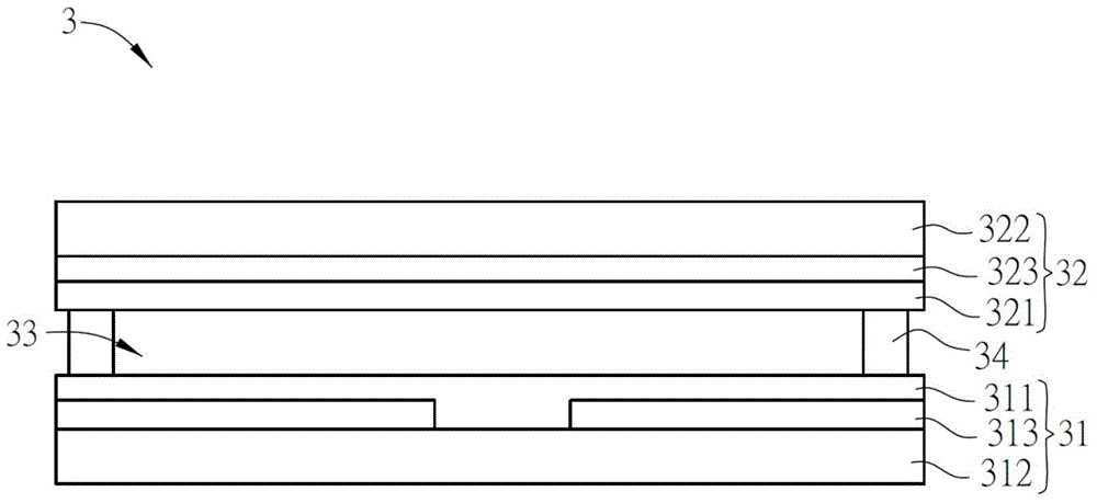
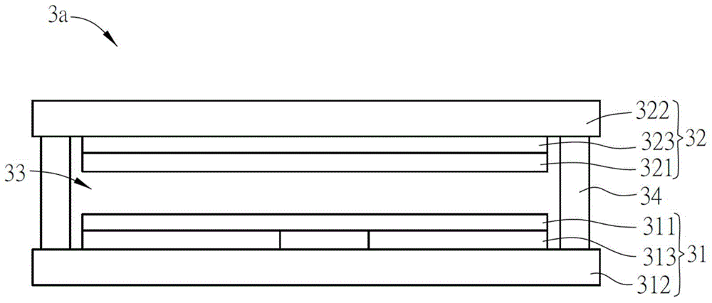
[0052] The exposure system can perform an exposure process on an assembly liquid crystal cell, so that the photoreactive monomers in the liquid crystal in the assembled liquid crystal panel can be polymerized into a polymer alignment layer that can control the liquid crystal alignment. The so-called "assembled liquid crystal panel" here refers to a panel that has completed the filling and assembly of the upper and lower substrates and the liquid crystal layer, but has not been cut to become a single display panel product. Wherein, an assembled liquid crystal panel may contain one display panel (including a set of upper and lower substrates and a liquid crystal layer), or multiple sets of display panels (including multiple sets of u...


PUM


Abstract

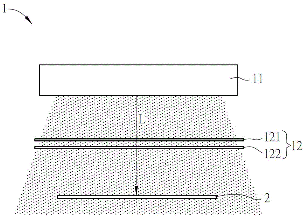
The invention discloses an exposure system and an exposure process. The exposure system carries out the exposure process on an assemblage liquid crystal display panel. Time for continuous exposure which should be carried out is set for the assemblage liquid crystal display panel. The exposure system comprises a light source device, a shutter device and a control device. The light source device can emit light to irradiate on the assemblage liquid crystal display panel. The shutter device is located on a light path of the light. The control device controls the light source device or the shutter device to further control light source illumination irradiated on the assemblage liquid crystal display panel. The control device enables the assemblage liquid crystal display panel in the exposure process to have a plurality of first exposure time periods for receiving the first light source illumination and a plurality of second exposure time periods for receiving the second light source illumination. The first exposure time periods and the second exposure time periods are arranged in a staggered mode. The sum of the first exposure time periods and the second exposure time periods is essentially equal to the time for continuous exposure which should be carried out.

Description

technical field [0001] The invention relates to an exposure system and an exposure process, in particular to an exposure system and an exposure process for assembling a liquid crystal panel. Background technique [0002] With the advancement of technology, flat panel display devices have been widely used in various fields, especially liquid crystal display devices, which have gradually replaced traditional cathode ray tube display devices due to their superior characteristics such as light and thin body, low power consumption and no radiation. , and applied to many kinds of electronic products, such as mobile phones, portable multimedia devices, notebook computers, LCD TVs and LCD screens, etc. [0003] At present, manufacturers of liquid crystal display devices are improving the wide viewing angle technology (Multi-domain Vertical Alignment, MVA) of thin-film transistor liquid crystal display devices (TFT LCD), polymer stable alignment (or polymer sustained alignment, Polym...

Claims


Application Information

Patent Timeline
Patent Type & Authority Applications(China)
IPC IPC(8): G02F1/1337G02F1/1333G03F7/20
CPCG02F1/133711G02F1/133788G03F7/2006G03F7/2022G02F1/133715
Inventor 林承叡陈右儒高振宽郑竹均
Owner INNOLUX CORP
Learn More