Organic electroluminescent device and preparation method thereof
An electroluminescent device and electroluminescent technology, which are applied in the fields of electro-solid devices, semiconductor/solid-state device manufacturing, electrical components, etc., and can solve the problems of short service life, poor mechanical strength, and weak water and oxygen resistance.
- Summary
- Abstract
- Description
- Claims
- Application Information
AI Technical Summary
Problems solved by technology
Method used
Image
Examples
Embodiment 1
[0081] An organic electroluminescent device is prepared through the following steps:
[0082] (1) Provide a clean anode conductive substrate:
[0083] Clean the ITO glass substrate sequentially with acetone, ethanol, deionized water, and ethanol in an ultrasonic cleaner for 5 minutes, then dry it with nitrogen, and dry it in an oven for later use; surface activation is performed on the cleaned ITO glass processing; ITO thickness is 100nm;
[0084] (2) Vacuum evaporation of the luminescent functional layer on the ITO glass substrate:
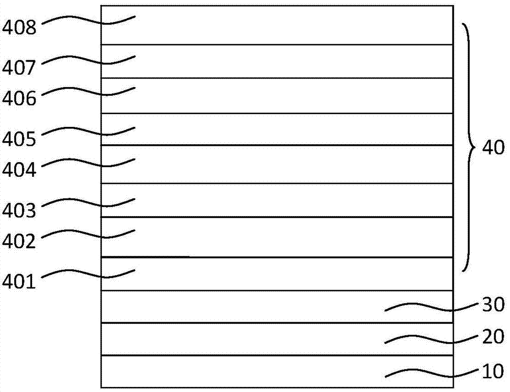
[0085] Specifically, the light emitting functional layer includes a hole injection layer, a hole transport layer, a light emitting layer, an electron transport layer and an electron injection layer;
[0086] Preparation of the hole injection layer: the MoO 3 The mixture obtained by mixing with NPB according to the mass ratio of 3:7 is used as the material of the hole injection layer, the thickness is 10nm, and the vacuum degree is 3×10 -5 Pa,...
Embodiment 2
[0099] An organic electroluminescent device is prepared through the following steps:
[0100] (1), (2), (3) are the same as embodiment 1;
[0101] (4) Prepare the encapsulation layer on the outside of the cathode:
[0102] The encapsulation layer is an organic barrier layer and an inorganic barrier layer alternately stacked 6 times;
[0103] Production of organic barrier layer: A layer of NPB was prepared on the cathode by vacuum evaporation, with a vacuum degree of 5×10 -5 Pa, evaporation rate Thickness 250nm;
[0104] Fabrication of inorganic barrier layer: combining Zr and Al 2 o 3 The mixture formed by mixing according to the mass ratio of 3:7 is used as the material of the inorganic barrier layer, which is produced by magnetron sputtering method, the acceleration voltage is 300V, the magnetic field is 200G, and the power density is 1W / cm 2 , the background vacuum is 1×10 -5 Pa, thickness 150nm;
[0105] Finally, an organic electroluminescence device is obtained. ...
Embodiment 3
[0107] An organic electroluminescent device is prepared through the following steps:
[0108] (1), (2), (3) are the same as embodiment 1;
[0109] (4) Prepare the encapsulation layer on the outside of the cathode:
[0110] The encapsulation layer is an organic barrier layer and an inorganic barrier layer alternately stacked 6 times;
[0111] Fabrication of organic barrier layer: prepare a layer of Alq on the cathode by vacuum evaporation3 , vacuum degree 5×10 -5 Pa, evaporation rate Thickness 200nm;
[0112] Fabrication of inorganic barrier layer: Hf and In 2 o 3 The mixture formed by mixing according to the mass ratio of 1:9 is used as the material of the inorganic barrier layer. It is produced by magnetron sputtering method, the accelerating voltage is 800V, the magnetic field is 50G, and the power density is 40W / cm 2 , background vacuum 5×10 -5 Pa, thickness 100nm;
[0113] Finally, an organic electroluminescence device is obtained.
PUM
| Property | Measurement | Unit |
|---|---|---|
| thickness | aaaaa | aaaaa |
| thickness | aaaaa | aaaaa |
| thickness | aaaaa | aaaaa |
Abstract
Description
Claims
Application Information
 - R&D
- Intellectual Property
- Life Sciences
- Materials
- Tech Scout
- Unparalleled Data Quality
- Higher Quality Content
- 60% Fewer Hallucinations
Browse by: Latest US Patents, China's latest patents, Technical Efficacy Thesaurus, Application Domain, Technology Topic, Popular Technical Reports.
© 2025 PatSnap. All rights reserved.Legal|Privacy policy|Modern Slavery Act Transparency Statement|Sitemap|About US| Contact US: help@patsnap.com


