
Texture pretreatment method for diamond wire cut polycrystalline silicon wafer, texturing pretreated silicon wafer and application thereof

A technology of diamond wire cutting and polysilicon wafers, which is applied in post-processing, post-processing details, chemical instruments and methods, etc. It can solve the problems of new cutting process silicon wafers that cannot be mass-produced, irregular suede surface, and low battery conversion efficiency. , to achieve the effect of simple pretreatment method, low reflectivity and short processing time

Active Publication Date: 2017-03-15
滁州赛维能源科技有限公司
View PDF18 Cites 0 Cited by
  • Summary
  • Abstract
  • Description
  • Claims
  • Application Information

AI Technical Summary

Problems solved by technology

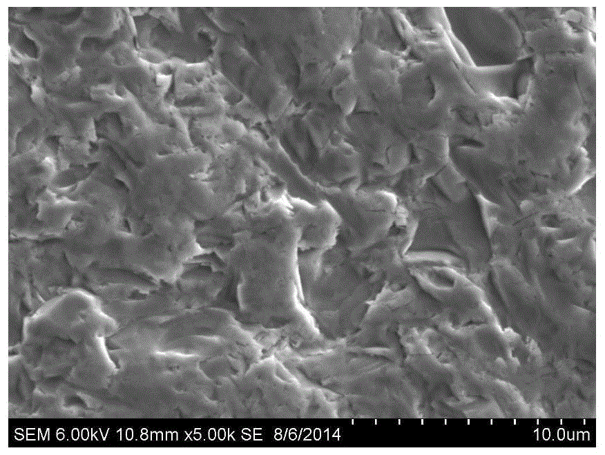
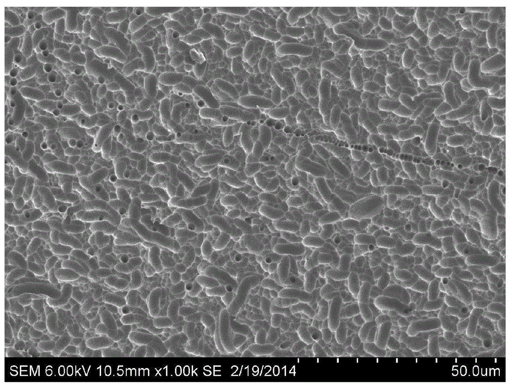
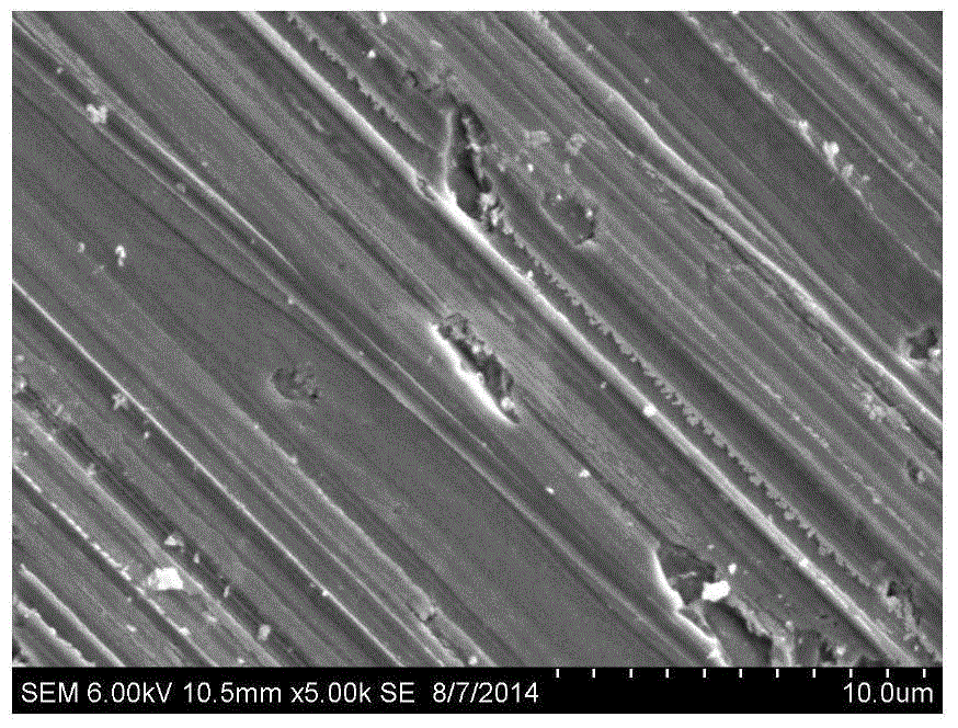
[0004] The surface damage layer of polycrystalline silicon wafers cut by conventional mortar is relatively uniform, about 10-11 μm, and there are no obvious line marks on the surface (such as figure 1 Shown), through the RENA process texturing process, that is, HF-HNO 3 -H 2 O acid velvet, can get the velvet surface with uniform corrosion on the whole surface (such as figure 2 shown); however, the surface damage layer of diamond wire-cut polysilicon wafers is relatively shallow, about 5-6 μm, and its damage is mainly caused by some small deep hole damage, and the surface is densely covered with smooth cutting line marks (such as image 3 shown); if the RENA texturing process of normal polysilicon wafers is used, the textured surface formed is very irregular and shallow (such as Figure 4 As shown), the reflectivity is much higher than that of normal silicon wafers, and its cell conversion efficiency is relatively low, which makes the new cutting process silicon wafers unable to be mass-produced

Method used


Image

  • Texture pretreatment method for diamond wire cut polycrystalline silicon wafer, texturing pretreated silicon wafer and application thereof
  • Texture pretreatment method for diamond wire cut polycrystalline silicon wafer, texturing pretreated silicon wafer and application thereof
  • Texture pretreatment method for diamond wire cut polycrystalline silicon wafer, texturing pretreated silicon wafer and application thereof

Examples


Embodiment 1

[0052] A kind of texturing pretreatment method of diamond wire cut polysilicon chip, comprises the steps:

[0053] (1) Take the polycrystalline silicon chip cut by diamond wire, clean it with a dilute HF solution with a mass concentration of 10%, and dry it, then place the silicon chip in a diffusion furnace, and heat up the diffusion furnace to 880 ° C. Inject large-flow nitrogen gas to remove the gas in the furnace, among which, the flow rate of large-flow nitrogen gas is 800ml / min;

[0054] (2) After the temperature of the diffusion furnace is stabilized, feed nitrogen and oxygen carrying a liquid phosphorus source for diffusion. The diffusion temperature is 880° C., and the diffusion time is 12 minutes. Wherein, the flow rate of nitrogen carrying a liquid phosphorus source is 60ml / min. The flow rate of oxygen is 40ml / min;

[0055] (3) Lead the diffusion furnace into a large flow of nitrogen to complete the diffusion process, and obtain a polysilicon wafer with a phosphoru...

Embodiment 2

[0062] A kind of texturing pretreatment method of diamond wire cut polysilicon chip, comprises the steps:

[0063] (1) Take the polysilicon wafer cut by diamond wire, wash it with a dilute HF solution with a mass concentration of 5%, and dry it, then place the silicon wafer in a diffusion furnace, and heat the diffusion furnace to 850°C, Inject large-flow nitrogen gas to remove the gas in the furnace, among which, the flow rate of large-flow nitrogen gas is 500ml / min;

[0064] (2) After the temperature of the diffusion furnace is stabilized, feed nitrogen and oxygen carrying a liquid phosphorus source for diffusion. The diffusion temperature is 850° C., and the diffusion time is 10 minutes. Wherein, the flow rate of nitrogen carrying a liquid phosphorus source is 40ml / min. The flow rate of oxygen is 30ml / min;

[0065] (3) Leading the diffusion furnace into a large flow of nitrogen gas to complete the diffusion process to obtain a polysilicon wafer with a phosphorus diffusion ...

Embodiment 3

[0071] A kind of texturing pretreatment method of diamond wire cut polysilicon chip, comprises the steps:

[0072] (1) Take the polysilicon wafer cut by diamond wire, wash it with a dilute HF solution with a mass concentration of 20%, remove the oil stain and oxide layer on the surface of the silicon wafer, and dry it, then place the silicon wafer in a diffusion furnace , and raise the temperature of the diffusion furnace to 900°C, feed a large flow of nitrogen gas to remove the gas in the furnace, wherein the flow rate of the large flow nitrogen gas is 1000ml / min;

[0073] (2) After the temperature of the diffusion furnace is stabilized, feed nitrogen and oxygen carrying a liquid phosphorus source for diffusion. The diffusion temperature is 900° C., and the diffusion time is 15 minutes. Wherein, the flow rate of nitrogen carrying a liquid phosphorus source is 100 ml / min. The flow rate of oxygen is 90ml / min;

[0074] (3) Leading the diffusion furnace into a large flow of nitr...


PUM

PropertyMeasurementUnit
reflectanceaaaaaaaaaa

Abstract

The invention provides a texturing preprocessing method of a diamond wire cut polycrystalline silicon chip. The method comprises the following step of preprocessing the diamond wire cut polycrystalline silicon chip by phosphorus diffusion under the temperature of 850 to 900 DEG C to form an N type heavily-doped layer with square resistance of 40 to 100 ohm / Sq on the surface layer of the silicon chip so as to obtain a textured preprocessed silicon chip. The invention further provides a texturing method of the diamond wire cut polycrystalline silicon chip. The textured preprocessed silicon chip is textured generally to form a uniform and low-reflectivity textured surface so as to obtain the diamond wire cut polycrystalline silicon chip textured product. The invention also provides the textured preprocessed silicon chip and the diamond wire cut polycrystalline silicon chip textured product.

Description

technical field [0001] The invention belongs to the technical field of texturing of polycrystalline silicon wafers, and in particular relates to a diamond wire-cut polycrystalline silicon wafer texturing pretreatment method, texturing pretreated silicon wafers and applications thereof. Background technique [0002] Silicon wafers are widely used in photovoltaic solar energy, liquid crystal display and semiconductor fields, so the technology of cutting silicon blocks to make silicon wafers has also been developed. At present, the cutting of crystalline silicon wafers used in the photovoltaic industry mainly adopts the mortar multi-wire cutting technology, but this technology has problems such as low cutting process efficiency, high cost, and large discharge pollution of waste mortar after cutting. In contrast, solid abrasive diamond wire saw cutting (referred to as diamond wire cutting) technology has the characteristics of fast cutting speed, high cutting precision, low mate...

Claims


Application Information

Patent Timeline
Patent Type & Authority Patents(China)
IPC IPC(8): C30B33/10H01L31/18
CPCY02P70/50
Inventor 章金兵彭也庆付红平
Owner 滁州赛维能源科技有限公司
Learn More