Method for manufacturing embedded source/drain MOS transistors

A technology of MOS transistors and manufacturing methods, which is applied in the field of manufacturing embedded source/drain MOS transistors, can solve problems such as reducing the epitaxial growth rate of silicon germanium, and achieve the effect of preventing adhesion

Active Publication Date: 2015-03-25
SEMICON MFG INT (SHANGHAI) CORP
View PDF6 Cites 3 Cited by
  • Summary
  • Abstract
  • Description
  • Claims
  • Application Information

AI Technical Summary

Problems solved by technology

[0005] However, when the concentration of germanium in silicon germanium is increased in the groove where the source and drain of the PMOS transistor are formed, the number of silicon germanium particles Dot attached to the NMOS transistor will also increase, such as figure 2 as shown, figure 2 It is a schematic top view shown in Figure 1. After cleaning with acidic HCl (hydrogen chloride) gas, although the HCL gas reacts with the silicon germanium attached to the NMOS tube to generate a mixed gas to reduce particles, it will greatly reduce the epitaxial growth rate of silicon germanium.

Method used


Image

  • Method for manufacturing embedded source/drain MOS transistors
  • Method for manufacturing embedded source/drain MOS transistors
  • Method for manufacturing embedded source/drain MOS transistors

Examples


Embodiment 1

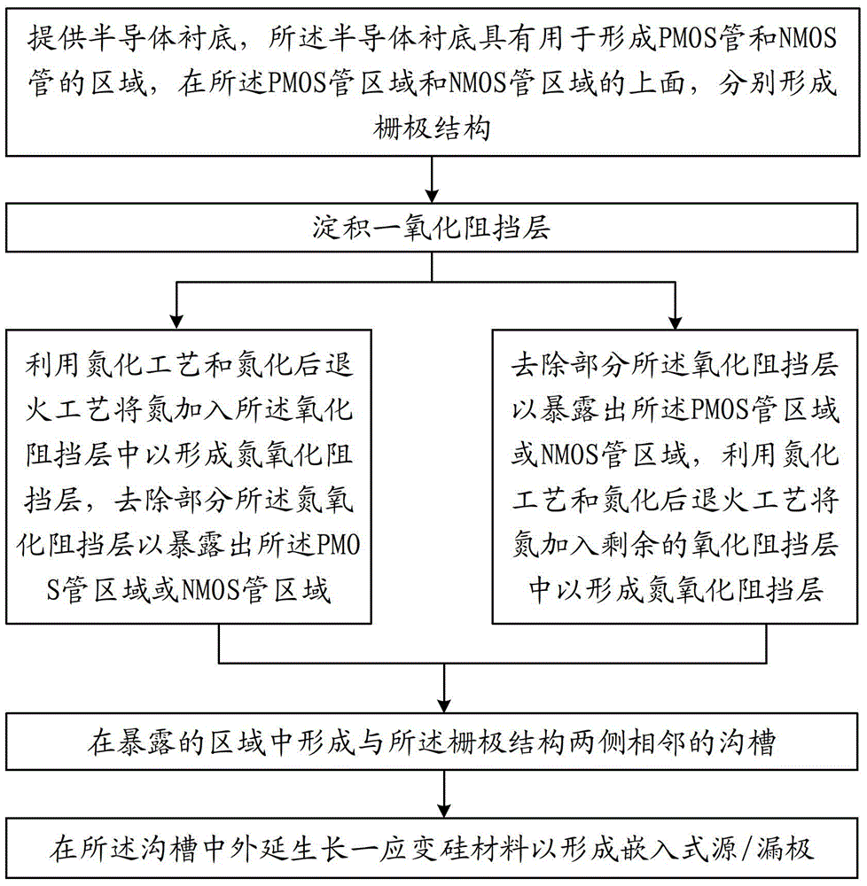
[0030] by figure 2 The manufacturing flow shown is an example, combined with Figure 3a to Figure 3f , a method for manufacturing an embedded source / drain MOS transistor provided by the present invention will be described in detail.

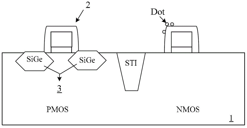
[0031] In step S1, see Figure 3a , provide a semiconductor substrate 10, the semiconductor substrate 10 has at least a region for forming a PMOS transistor and an NMOS transistor region, a gate structure 12 is formed on the PMOS transistor region, and also in the NMOS transistor region The same gate structure 12 is also formed above. The gate structure 12 includes a gate oxide layer 12-1, a polysilicon gate 12-2 located on the semiconductor substrate from bottom to top, and a gate side surrounding the gate oxide layer 12-1 and the polysilicon gate 12-2. Wall 12-3.

[0032] Further, a shallow trench isolation (STI) for insulating the PMOS transistor region and the NMOS transistor region is also formed on the semiconductor substrate 10 .

[0...

Embodiment 2

[0040] by figure 2 The manufacturing flow shown is an example, combined with Figure 3a-3b and 3g to Figure 3j , a method for manufacturing an embedded source / drain MOS transistor provided by the present invention will be described in detail.

[0041] The contents in steps S1 and S2 in this embodiment are the same as those in steps S1 and S2 in the first embodiment, and will not be repeated here. For specific contents and corresponding parameters, please refer to step S1 in the first embodiment , S2.

[0042] In step S3, see Figure 3g , taking the NMOS tube area as an example, the oxidation barrier layer 14 covering the NMOS tube area to be exposed is removed to expose the NMOS tube area, while the unremoved oxidation barrier layer 14 still covers the PMOS tube area.

[0043] Then, see Figure 3h , using DPN technology to add nitrogen into the remaining oxidation blocking layer 14 , and then using PNA technology to stabilize the nitrogen added to the oxidation blocking ...


PUM


Abstract

The invention provides a method for manufacturing embedded source / drain MOS transistors. The method comprises the steps that gate structures are formed on a PMOS transistor area and an NMOS transistor area formed on a semiconductor substrate respectively; an oxidation barrier layer is deposited; through a nitriding technology and a post-nitridation annealing technology, nitrogen is added to the oxidation barrier layer to form a nitrogen oxidation barrier layer, and a part of the nitrogen oxidation barrier layer is removed to expose the PMOS transistor area or the NMOS transistor area, or after a part of the oxidation barrier layer is removed to expose the PMOS transistor area or the NMOS transistor area, nitrogen is added to the remaining oxidation barrier layer to form the nitrogen oxidation barrier layer through the nitriding technology and the post-nitridation annealing technology; channels adjacent to the two sides of each gate structure are formed in the exposed area; strained silicon materials grow in the channels in an epitaxial mode to form the embedded source / drain MOS transistors. According to the method, the rate of epitaxial growth of the strained silicon materials in the channels is guaranteed, and the risk of pollution to the embedded source / drain MOS transistors can be lowered through the remaining oxidation barrier layer.

Description

technical field [0001] The invention belongs to the technical field of semiconductor integrated circuit manufacturing, and in particular relates to a manufacturing method of an embedded source / drain MOS transistor. Background technique [0002] The size of MOS transistors (Metal Oxide Semiconductor Field Effect Transistors) has been continuously reduced over the past few decades. In early semiconductor circuit technology, the channel length in MOS transistors was on the order of several microns. By the end of the 1990s, the size of MOS transistors continued to shrink, which greatly improved the performance of semiconductor circuits. In today's semiconductor circuit technology, this parameter has been reduced by dozens of times or even more than one hundred times. [0003] However, the reduction in the size of MOS transistors also brings some negative problems. For example, a smaller channel width increases the channel equivalent resistance. Therefore, for MOS transistors...

Claims


Application Information

Patent Timeline
IPC IPC(8): H01L21/8238H01L21/336
CPCH01L21/02109H01L29/401H01L29/66477H01L29/7845H01L29/7848H01L29/84
Inventor 禹国宾刘海龙
Owner SEMICON MFG INT (SHANGHAI) CORP
Why Eureka
Try Eureka