


Quick Research
Generate reliable direction feasibility study reports for your R&D in just a few steps.

Technical Q&A
Discover and master advanced knowledge NOW. Basics, ideas, possibilities, all at once.

Find Solutions
As an expert in R&D theories, this can generate solutions to your technical problems instantly.

Evaluate Feasibility
Analyze your overall solution with one click, know your potential R&D risks in advance.

Monitor Landscape
Get weekly tech updates, stay abreast of the latest tech innovations and key insights.
Preparation method of polysilicon thin film material
A technology of polycrystalline silicon thin film and amorphous silicon thin film, which is applied in the manufacture of semiconductor/solid-state devices, electrical components, circuits, etc., can solve the problems of lowering the crystallization temperature of the film, shortening the time required for crystallization, and large laser energy, and saving energy Energy, laser threshold energy reduction, effect of low process temperature
- Summary
- Abstract
- Description
- Claims
- Application Information
AI Technical Summary
Problems solved by technology
Method used
Image


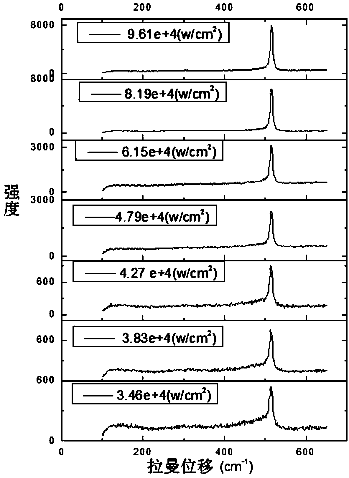
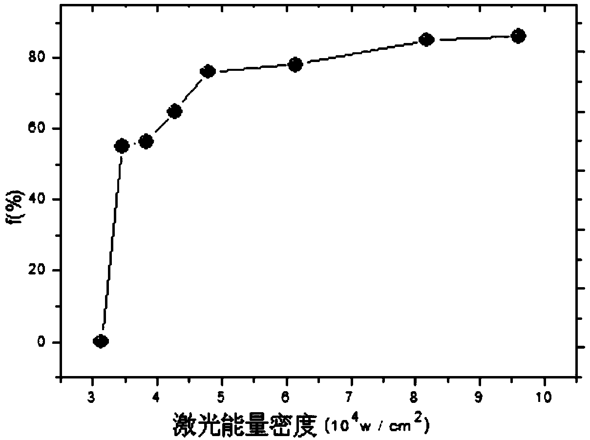
Examples
Embodiment 1
[0039] Such asfigure 1 As shown, a layer of amorphous silicon thin film 2 is deposited on a glass substrate 1 using an intrinsic silicon target with a purity of 99.999% by magnetron sputtering technology. The specific process conditions are: the deposition pressure is 1Pa, the glow power is 80W, The flow rate of argon gas is 26 sccm, the substrate temperature is 150° C., and the deposition time is 30 minutes to obtain an amorphous silicon film 2 with a thickness of 360 nm;
[0040] After the deposition of the amorphous silicon film 2 is completed, a metal aluminum film 3 is sputtered and deposited on the amorphous silicon film 2 in the same vacuum chamber using an aluminum target with a purity of 99.999%. The process conditions are as follows: the deposition pressure is 1 Pa, The optical power is 60W, the flow rate of argon gas is 26sccm, the substrate temperature is 100°C, and the coating time is 2min, and a metal aluminum film 3 with a thickness of 22nm is obtained;
[0041]...
Embodiment 2
[0047] Such as figure 1 As shown, a layer of amorphous silicon thin film 2 is deposited on a glass substrate 1 using an intrinsic silicon target with a purity of 99.9999% by magnetron sputtering technology. The specific process conditions are: the deposition pressure is 0.8Pa, and the glow power is 80W. , the flow rate of argon gas is 20 sccm, the substrate temperature is 150° C., and the deposition time is 25 minutes to obtain an amorphous silicon film 2 with a thickness of 325 nm;
[0048] After the deposition of the amorphous silicon film 2 is completed, a metal aluminum film 3 is deposited on the amorphous silicon film 2 by sputtering with an aluminum target with a purity of 99.9999% in the same vacuum chamber. The process conditions are as follows: the deposition pressure is 1 Pa, The optical power is 80W, the flow rate of argon gas is 20sccm, the substrate temperature is 150°C, and the coating time is 1.5min, to obtain a metal aluminum film 3 with a thickness of 18nm;
...
Embodiment 3
[0054] Such as figure 1 As shown, a layer of amorphous silicon thin film 2 is deposited on a glass substrate 1 using an intrinsic silicon target with a purity of 99.9999% by magnetron sputtering technology. The specific process conditions are: the deposition pressure is 2.0Pa, and the glow power is 60W , the flow rate of argon gas is 30 sccm, the substrate temperature is 100° C., and the deposition time is 36 minutes to obtain an amorphous silicon thin film 2 with a thickness of 360 nm;
[0055] After the deposition of the amorphous silicon film 2 is completed, a metal aluminum film 3 is sputtered and deposited on the amorphous silicon film 2 in the same vacuum chamber using an aluminum target with a purity of 99.9999%. The process conditions are as follows: the deposition pressure is 2Pa, The optical power is 40W, the flow rate of argon gas is 30sccm, the substrate temperature is 100°C, and the coating time is 40s to obtain a metal aluminum film 3 with a thickness of 6nm;
...
PUM
| Property | Measurement | Unit |
|---|---|---|
| wavelength | aaaaa | aaaaa |
| diameter | aaaaa | aaaaa |
| thickness | aaaaa | aaaaa |
Abstract
Description
Claims
Application Information
 - R&D Engineer
- R&D Manager
- IP Professional
- Industry Leading Data Capabilities
- Powerful AI technology
- Patent DNA Extraction
Browse by: Latest US Patents, China's latest patents, Technical Efficacy Thesaurus, Application Domain, Technology Topic, Popular Technical Reports.
© 2024 PatSnap. All rights reserved.Legal|Privacy policy|Modern Slavery Act Transparency Statement|Sitemap|About US| Contact US: help@patsnap.com