Eureka AIR delivers breakthrough ideas for toughest innovation challenges, trusted by R&D personnel around the world.

Reaction device and preparation method of nitrogen doped silicon carbide film

A technology of reaction equipment and silicon carbide, which is applied in gaseous chemical plating, semiconductor/solid-state device manufacturing, coating, etc., can solve problems such as enhanced adhesion, increased K value, and decreased adhesion, so as to improve reliability and Electrical performance, improvement of process quality, and effect of enhancing adhesion

Inactive Publication Date: 2014-12-03
SHANGHAI HUALI MICROELECTRONICS CORP
View PDF3 Cites 2 Cited by
  • Summary
  • Abstract
  • Description
  • Claims
  • Application Information

AI Technical Summary

Problems solved by technology

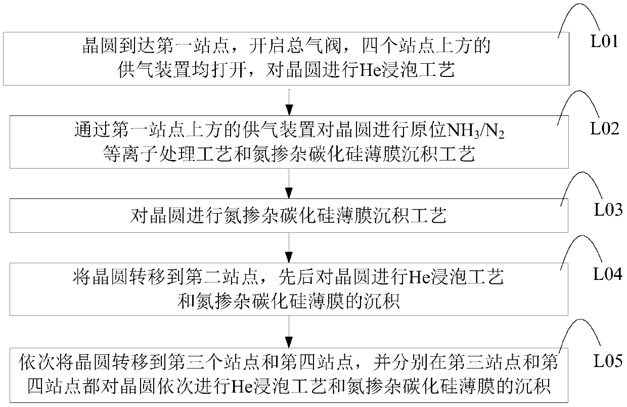
[0010] In the preparation method of the above-mentioned nitrogen-doped silicon carbide film, both He Soak and in-situ NH 3 / N 2 The pretreatment of the plasma treatment process, and the deposition process of the nitrogen-doped silicon carbide film, will affect the effectiveness of the pretreatment process due to the inevitable occurrence of a mixed atmosphere: if the pretreatment process cannot remove the CuO on the Cu surface Effective removal will lead to a decrease in the adhesion of Cu and nitrogen-doped silicon carbide films, thereby affecting the reliability of the final device; and the pretreatment process will affect the K value of the porous low k dielectric, as well as the low k material and The adhesion of nitrogen-doped silicon carbide film, if the K value of the low k dielectric cannot be effectively repaired during the pretreatment process, and the adhesion between the low k material and the nitrogen-doped silicon carbide film cannot be enhanced, the K value will increase. High, which affects the electrical performance and reliability of the final device

Method used


Image

  • Reaction device and preparation method of nitrogen doped silicon carbide film
  • Reaction device and preparation method of nitrogen doped silicon carbide film
  • Reaction device and preparation method of nitrogen doped silicon carbide film

Examples


Embodiment Construction

[0030] In order to make the content of the present invention clearer and easier to understand, the content of the present invention will be further described below in conjunction with the accompanying drawings. Of course, the present invention is not limited to this specific embodiment, and general replacements known to those skilled in the art are also covered within the protection scope of the present invention.

[0031] In the present invention, the reaction equipment for nitrogen-doped silicon carbide film can adopt the existing reaction equipment for nitrogen-doped silicon carbide film, which has a reaction chamber, usually the reaction chamber has first, second, third and The fourth station, above each station, includes an air supply device, such as an air intake shower head, etc., there may be a transfer device between the four stations so that the wafers can be transferred between them, and there are also separate facilities in the reaction equipment. Control the radio f...


PUM


Abstract

The invention provides a reaction device and preparation method of a nitrogen doped silicon carbide film. An air feed device above a first station comprises an independent remote plasma system, for generating remote H2 / He plasma during a preprocessing process or remote NH3 / N2 plasma, for repairing the k value of a low k medium and removing CuO on the surface of Cu so as to enhance the adhesiveness of a low k material and the nitrogen doped silicon carbide film and the adhesiveness of the Cu and the nitrogen doped silicon carbide film; the air feed device above the first station is different from the air feed devices of other three stations and is independently controlled, such that the preprocessing process can be freely adjusted; since the four stations work simultaneously in a reaction cavity of the reaction device, for the purpose of eliminating mutual interference between the preprocessing process and other processes, the four stations are isolated by use of an gas curtain technology, and the technical quality of the preprocessing process is improved; and the reliability and the electrical performance of a final product can be improved.

Description

technical field [0001] The invention relates to the technical field of semiconductors, in particular to a reaction device for a nitrogen-doped silicon carbide film and a preparation method thereof. Background technique [0002] Nitrogen-doped silicon carbide film (NDC) is used as a barrier layer in the back-end process of integrated circuit manufacturing, the purpose is to prevent direct contact between filled copper and dielectric materials, and copper diffusion occurs. Such as figure 1 As shown, it is a schematic diagram of the structure after the deposition of low K dielectric material, usually after the chemical mechanical polishing (CMP) of copper filling 1, and before the deposition of low K dielectric 3, nitrogen is carried out by plasma enhanced chemical vapor deposition (PECVD) Deposition of doped silicon carbide film 2 . For technology nodes below 40nm, in order to meet K value requirements, low K media usually use porous low k media. Due to factors such as grin...

Claims


Application Information

Patent Timeline
Patent Type & Authority Applications(China)
IPC IPC(8): H01L21/3115C23C16/44C23C16/448
CPCC23C16/325C23C16/0245C23C16/45519H01L21/02167H01L21/02274
Inventor 雷通
Owner SHANGHAI HUALI MICROELECTRONICS CORP
Why Eureka
Eureka Blog
Learn More