
Method and lithography machine for judging consistency of overlay accuracy of lithography plate

A technique of engraving accuracy and photolithography, which is applied in the field of photolithography, can solve problems such as large impact, large manpower required, and long cycle time, and achieve low complexity, improve evaluation efficiency, and reduce evaluation difficulty. Effect

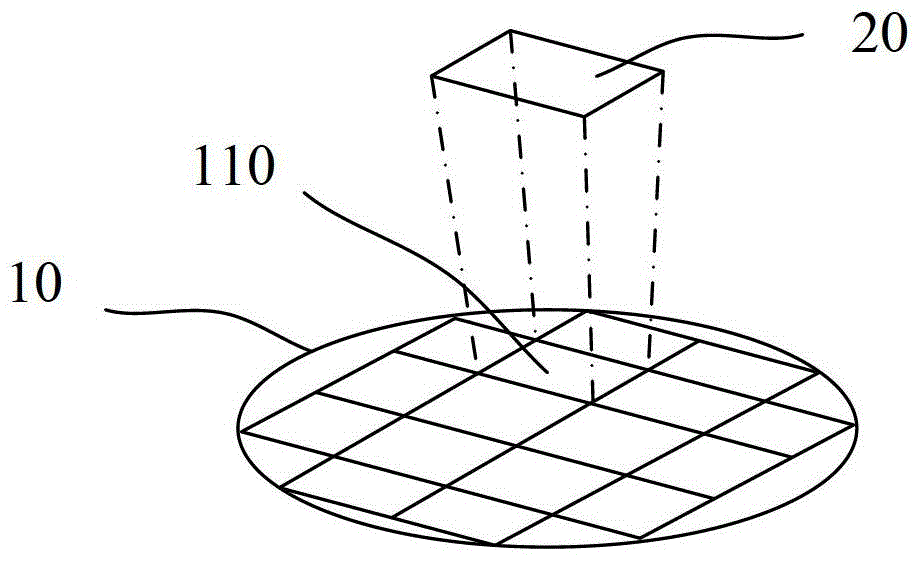
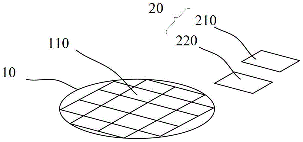
Active Publication Date: 2016-12-28
WUXI DISI MICROELECTRONICS CO LTD
View PDF6 Cites 0 Cited by
  • Summary
  • Abstract
  • Description
  • Claims
  • Application Information

AI Technical Summary

Problems solved by technology

[0005] The above method consumes a long cycle, requires a lot of manpower, and is greatly affected by the processes of other departments, so it is difficult to evaluate the consistency of overlay accuracy

Method used


Image

  • Method and lithography machine for judging consistency of overlay accuracy of lithography plate
  • Method and lithography machine for judging consistency of overlay accuracy of lithography plate
  • Method and lithography machine for judging consistency of overlay accuracy of lithography plate

Examples


Embodiment Construction

[0019] In the semiconductor manufacturing process, the photolithography process is a relatively critical process. The photolithography process includes steps such as pretreatment, spin-coating photoresist, soft baking, exposure, post-baking, and development. in:

[0020] 1) Substrate Pretreatment is used to change the properties of the wafer surface so that it can adhere firmly to the photoresist. The main method is to apply hexamethyldisilamine (HMDS): the wafer is heated to 120°C in a closed chamber, and the surface is sprayed with nitrogen to pressurize the mist of HMDS, so that the HMDS and the -OH bond on the wafer surface react. To remove water vapor and hydrophilic bond structure. Cool down on a cold plate after the reaction is complete.

[0021] 2) Spin coating photoresist (Spin coat), the uniformity and stability of the photoresist film can be improved by the spin coating method. The main substances in photoresist are resin, solvent, photosensitive agent and other...


PUM


Abstract

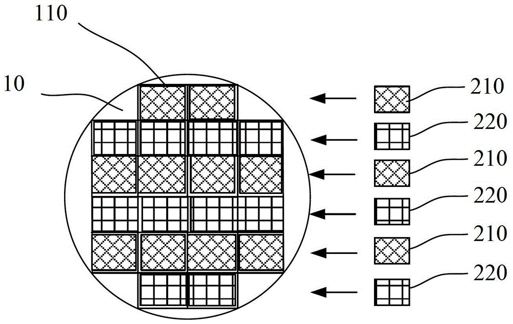
The invention discloses a method for judging the consistency of the overlay accuracy of photolithography plates. In the photolithography process, the following steps are included: using two photolithography plates to expose the surface of the wafer in the manner of row interval or column interval; Compare the entire wafer with the wafer exposed through a single photolithography plate to judge the consistency of overlay accuracy. Also disclosed is a photolithography machine applying the above method. The above method and photolithography machine can improve the evaluation efficiency and reduce the evaluation difficulty of judging the consistency of the overlay accuracy of the photolithography plate.

Description

technical field [0001] The invention relates to photolithography technology, in particular to a method for judging the consistency of overlay accuracy of a photolithography plate and a photolithography machine. Background technique [0002] When producing wafers, photolithography is required to transfer the pattern on the photolithography plate to the wafer. The pattern transferred each time occupies an area on the wafer. After multiple transfers, multiple regions with the same pattern can be formed on the wafer, and then the wafer can be divided into regions to obtain multiple regions with the same function. wafer. [0003] In order to improve production efficiency, there has been a technology of using two photolithography plates to work on the same wafer at the same time, that is, using two photolithography plates to work independently on different areas of the wafer at the same time, and finally complete the graphics of the entire wafer transfer printing. In theory, th...

Claims


Application Information

Patent Timeline
Patent Type & Authority Patents(China)
IPC IPC(8): G03F7/20H01L21/027
Inventor 陈辉
Owner WUXI DISI MICROELECTRONICS CO LTD
Learn More