
Silver nano column cluster array, as well as preparation method and application thereof

A technology of silver nanorods and pillar arrays, which is applied in the direction of nanotechnology, nanotechnology, nanotechnology for materials and surface science, etc., can solve problems such as excessive silver nanorod spacing, high SERS activity, and preparation methods that cannot be solved. Achieve the effect of good uniformity and repeatability, good uniformity and repeatability, and simple preparation method

Inactive Publication Date: 2014-10-15
HEFEI INSTITUTES OF PHYSICAL SCIENCE - CHINESE ACAD OF SCI
View PDF6 Cites 16 Cited by
  • Summary
  • Abstract
  • Description
  • Claims
  • Application Information

AI Technical Summary

Problems solved by technology

Although this product has high SERS activity, the uniformity and repeatability of the signal are unsatisfactory because the silver nanorods are too long to keep the top of the original array neat and uniform, and the spacing of the silver nanorods is too large. too large to obtain higher SERS activity; in addition, the preparation method cannot solve the above-mentioned problems

Method used


Image

  • Silver nano column cluster array, as well as preparation method and application thereof
  • Silver nano column cluster array, as well as preparation method and application thereof

Examples


Embodiment 1

[0037] The concrete steps of preparation are:

[0038] Step 1, first transfer the single-layer crystal template with a ball diameter of 1.5 μm to the surface of a through-hole alumina template with a hole diameter of 55 nm; wherein, the single-layer crystal template is a polystyrene colloidal sphere template (or a silica microsphere template ) to get the composite template. A gold film with a thickness of 50 nm is sputtered on one side of the composite template with a single-layer crystal template to obtain a composite template covered with a gold film on one side.

[0039] Step 2, first place the composite template with a gold film on one side in the silver electrolyte, at a current density of 70 μA / cm 2 Electrodeposited at a constant current for 15 minutes to obtain a composite template with a gold film on one side and silver nanopillars in the holes. Then use chemical (or physical) method to remove the single-layer crystal template in the composite template; wherein, the ...

Embodiment 2

[0042] The concrete steps of preparation are:

[0043] Step 1, first transfer the single-layer crystal template with a ball diameter of 1.8 μm to the surface of a through-hole alumina template with a pore diameter of 60 nm; wherein, the single-layer crystal template is a polystyrene colloidal sphere template (or a silicon oxide microsphere template ) to get the composite template. A gold film with a thickness of 53 nm was sputtered on one side of the composite template with a single-layer crystal template to obtain a composite template covered with a gold film on one side.

[0044] Step 2, first place the composite template with a gold film on one side in the silver electrolyte, at a current density of 130μA / cm 2 Electrodeposited at a constant current for 14 minutes to obtain a composite template with a gold film on one side and silver nanopillars in the holes. Then use chemical (or physical) method to remove the single-layer crystal template in the composite template; where...

Embodiment 3

[0047] The concrete steps of preparation are:

[0048] Step 1, first transfer the single-layer crystal template with a ball diameter of 2 μm to the surface of a through-hole alumina template with a hole diameter of 65 nm; wherein, the single-layer crystal template is a polystyrene colloidal sphere template (or a silica microsphere template) , to get the composite template. A gold film with a thickness of 55 nm is sputtered on the side of the composite template with a single-layer crystal template to obtain a composite template covered with a gold film on one side.

[0049] Step 2, first place the composite template with a gold film on one side in the silver electrolyte, at a current density of 190μA / cm 2 Electrodeposited at a constant current for 13 minutes to obtain a composite template with a gold film on one side and silver nanopillars in the holes. Then use chemical (or physical) method to remove the single-layer crystal template in the composite template; wherein, the c...


PUM


Abstract

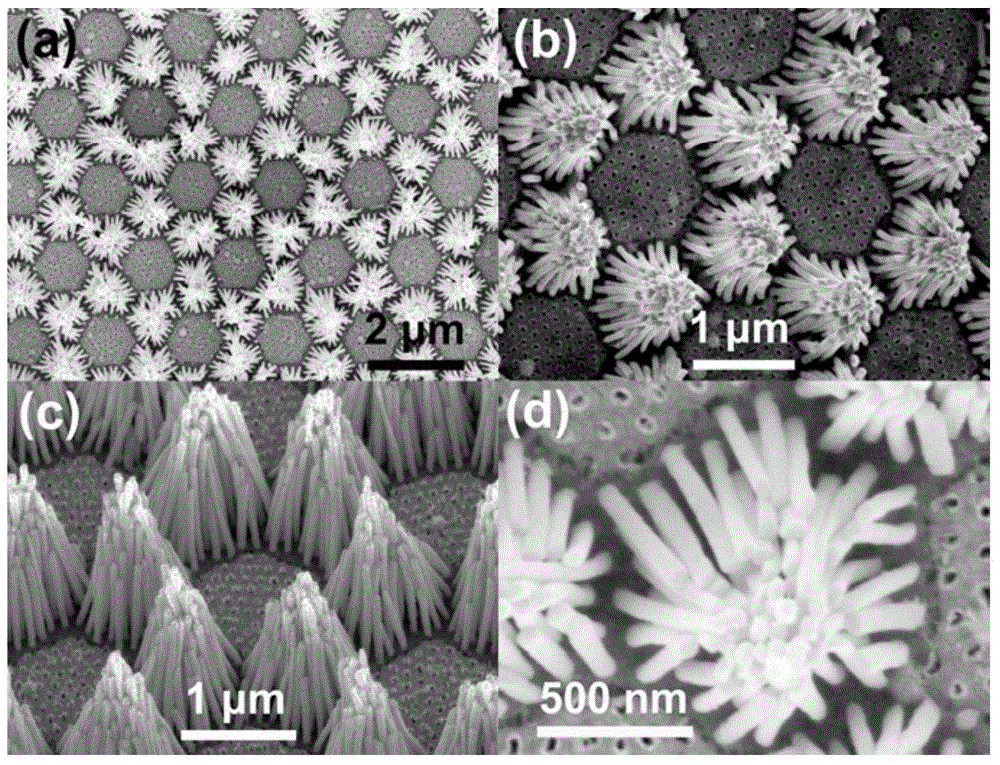
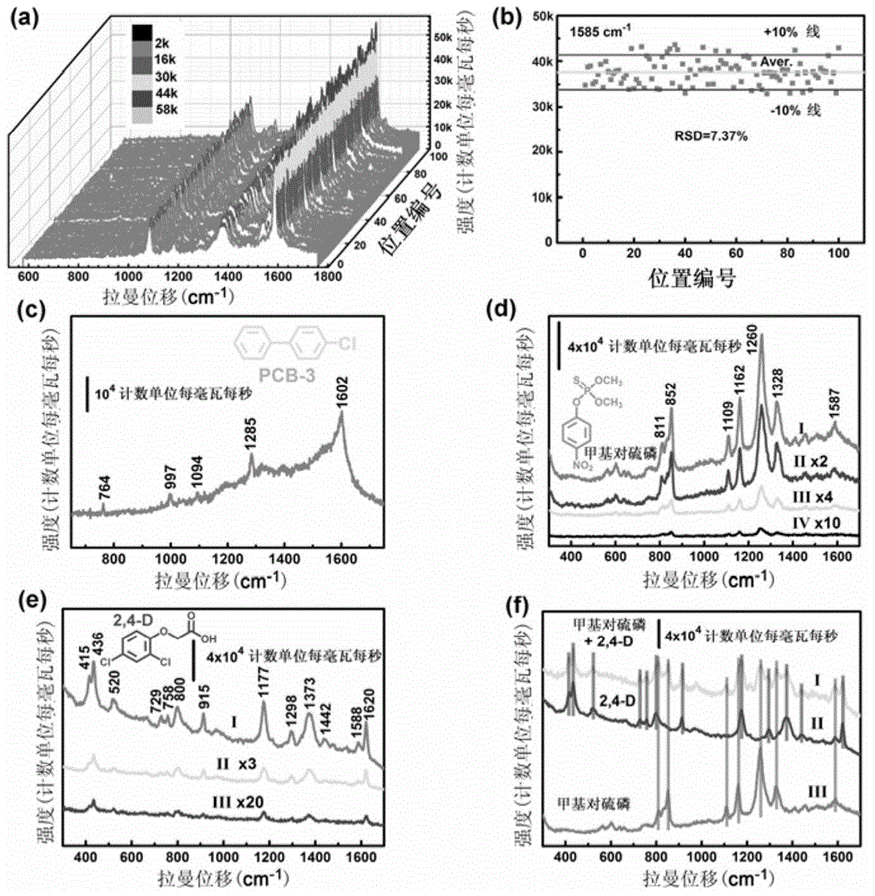
The invention discloses a silver nano column cluster array, as well as a preparation method and application thereof. The silver nano column cluster array comprises the silver nano column clusters covering a gold film, wherein the silver nano column clusters constituting the silver nano column cluster array comprises more than 20 silver nano columns; the diameter and length of each silver nano column are 5-75 nm and 750-850 nm respectively, the distance between the centers of the roots of two columns is 130-170 nm, and the top ends of the more than 20 columns are gathered. The preparation method comprises the following steps: a monolayer crystal template is moved to the surface of a through-hole alumina template, the gold film is sputtered on the monolayer crystal template, then, the monolayer crystal template is placed in a silver electrolyte, the monolayer crystal template is removed after the silver nano columns is subjected to electro-deposition, after the gold film is sputtered on one surface, covering the gold film, of the alumina template, the alumina template is dissolved away, and then the gold film on which the silver nano column cluster array is placed is dried to prepare the objective product, wherein one surface of the alumina template is coated with the gold film, and the silver nano columns are placed in the through holes of the alumina template. The silver nano column cluster array can be used as the active substrate of surface reinforced raman scattering, and a laser Raman spectrometer is utilized to measure polychlorinated biphenyl-3 attached thereon or measure the content of parathion-methyl in an organophosphorus pesticide or the content of 2, 4-D in an organo-chlorine pesticide.

Description

technical field [0001] The invention relates to a cluster array, its preparation method and application, in particular to a silver nanocolumn cluster array, its preparation method and application. Background technique [0002] Surface-enhanced Raman scattering (SERS) spectroscopy is one of the most sensitive analytical techniques that can provide fingerprint information of molecular vibrations and even enable single-molecule detection. Therefore, SERS technology has a wide range of applications in the fields of analytical chemistry, biochemistry, biomedicine, environmental monitoring and food safety testing. At present, for the application of SERS detection technology, one of the key problems to be solved is to prepare substrates with high SERS activity, good signal uniformity and repeatability. To this end, people have made unremitting efforts, such as a silver nanorod array modified by the applicant with mercapto-β-cyclodextrin and its preparation method published on Nove...

Claims


Application Information

Patent Timeline
IPC IPC(8): C23C14/18C23C28/02C25D3/46C25D5/48B82Y30/00B82Y40/00
Inventor 朱储红孟国文李中波
Owner HEFEI INSTITUTES OF PHYSICAL SCIENCE - CHINESE ACAD OF SCI
Learn More