
Semiconductor-wafer-surface-protective adhesive tape

An adhesive tape and semiconductor technology, which is applied in semiconductor devices, thin film/sheet adhesives, semiconductor/solid device manufacturing, etc. It can solve the problem of different adhesives, and it is difficult to improve the adhesion and prevent adhesives at the same time. , Peel off bad wafers and other problems, to achieve the effect of easy peeling

Active Publication Date: 2014-10-08
FURUKAWA ELECTRIC CO LTD
View PDF13 Cites 9 Cited by
  • Summary
  • Abstract
  • Description
  • Claims
  • Application Information

AI Technical Summary

Problems solved by technology

[0010] However, the UV-curable surface protection tape requires an ultraviolet irradiation process, so the process management is cumbersome, and its reactivity is high, so it often reacts with the active surface of the semiconductor wafer that has been specially surface-treated to cause poor peeling or chip cracking problem
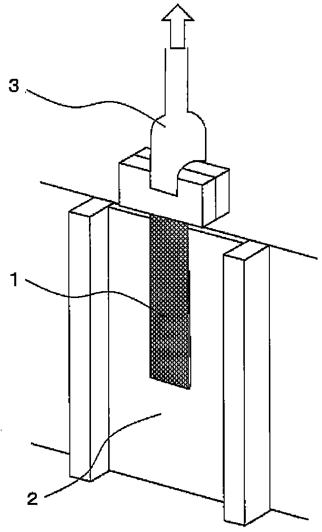
On the other hand, in the surface protection tape using pressure-sensitive adhesive, the adhesive cannot be cured by ultraviolet radiation, so it is difficult to improve the adhesion and prevent the adhesive from remaining, and it is difficult to apply to the discrete type. Devices with large step differences, bump wafers and other devices with bumps
[0011] In order to solve these problems, methods such as using two layers of adhesives or using resin in the middle layer to ensure adhesion have been considered, but if the adhesive that is in contact with the adherend is not UV-curable, then It is difficult to suppress the occurrence of adhesive residue, or when using a pressure-sensitive adhesive, it is necessary to clean the adherend
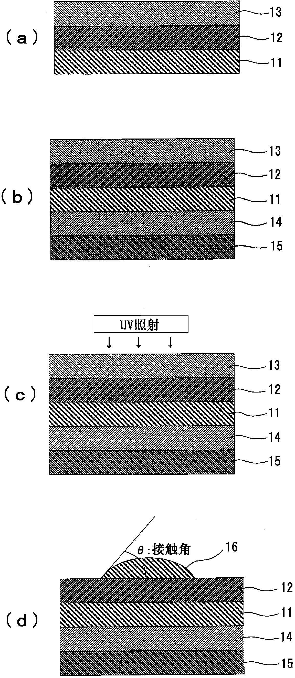
[0012] In view of these problems, by further adjusting the value of the contact angle to diiodomethane to solve the problem in the ultraviolet curable adhesive (see Patent Document 4), or to seek a solution to the problem in the same way for the pressure-sensitive adhesive ( Referring to Patent Document 5), however, the problem of adhesive residue due to differences in wafer surface conditions or differences in the depth or shape of unevenness such as scribe lines cannot be completely solved.

Method used


Image

  • Semiconductor-wafer-surface-protective adhesive tape
  • Semiconductor-wafer-surface-protective adhesive tape
  • Semiconductor-wafer-surface-protective adhesive tape

Examples


Embodiment

[0143] Hereinafter, the present invention will be described in more detail based on examples, but the present invention is not limited to these examples.

[0144]

[0145] A polyoxyethylene alkylphenyl ether compound to which an allyl group was added and a polypropylene glycol compound were added as surfactants to deionized pure water, ammonium persulfate was added as a polymerization initiator, and the mixture was stirred while heating. Then, 17 mass parts of methyl methacrylate, 40 mass parts of n-butyl acrylate, 41 mass parts of 2-ethylhexyl acrylate, 2 mass parts of glycidyl methacrylate were added dropwise in the stirring solution, Further, stirring was continued to perform polymerization, and an acrylic emulsion pressure-sensitive adhesive composition was obtained.

[0146] Coating and drying the adhesive composition on a polyethylene terephthalate (PET) release film of 25 μm, and laminating it on an ethylene-vinyl acetate copolymer (EVA) film having a thickness of 120...

Embodiment 2

[0148] In Example 1, the amount of methyl methacrylate was changed to 30 parts by mass, the amount of n-butyl acrylate was changed to 39 parts by mass, and the amount of 2-ethylhexyl acrylate was changed to 39 parts by mass. The adhesive tape for semiconductor wafer surface protection was produced similarly to Example 1 except having changed the film thickness of the adhesive layer into 48 micrometers.

Embodiment 3

[0150] In Example 1, the usage-amount of methyl methacrylate was changed to 16 parts by mass, the usage-amount of 2-ethylhexyl acrylate was changed to 40 parts by mass, and 2 parts by mass of methacrylic acid was further added, except Except for this, an acrylic emulsion pressure-sensitive adhesive composition was obtained in the same manner as in Example 1.

[0151]Except that the thickness of the EVA film was changed to 165 μm, and the film thickness of the adhesive layer was changed to 41 μm, this acrylic emulsion adhesive composition was made in the same manner as in Example 1 to produce an adhesive tape for semiconductor wafer surface protection. .


PUM

PropertyMeasurementUnit
Thicknessaaaaaaaaaa
Thicknessaaaaaaaaaa

Abstract

A semiconductor-wafer-surface-protective adhesive tape having a pressure-sensitive adhesive layer on a substrate film, wherein the thickness of the adhesive layer is 10mum or more, the surface free energy (gammas) of the surface of the adhesive layer is 30-35 mN / m, the contact angle (thetal I) in relation to diiodomethane is 54-60 DEG , the adhesive force in relation to an SUS280 polished surface at 23 DEG C is 0.8-4.3 N / 25mm, and the adhesive force in relation to the SUS280 polished surface when heat-releasing at 50 DEG C in comparison to the adhesive force when releasing at 23 DEG C is 50% or less.

Description

technical field [0001] The present invention relates to an adhesive tape (adhesive tape) for protecting the surface of a semiconductor wafer. More specifically, it is related with the adhesive tape for surface protection of the semiconductor wafer used when grinding a semiconductor wafer into a thin film. Background technique [0002] A semiconductor package is manufactured by slicing a high-purity silicon single crystal or the like into a semiconductor wafer, and then forming an integrated circuit on the surface of the wafer by ion implantation, etching, or the like. The semiconductor wafer has a desired thickness by grinding, polishing, or the like on the back surface of the semiconductor wafer on which the integrated circuit is formed. At this time, in order to protect the integrated circuit formed on the surface of the semiconductor wafer, an adhesive tape for protecting the surface of the semiconductor wafer is used. The semiconductor wafer subjected to backside grind...

Claims


Application Information

Patent Timeline
IPC IPC(8): C09J7/02C09J133/00C09J201/00H01L21/304
CPCC09J7/02C09J201/00C09J133/00H01L21/6836H01L21/304H01L2221/6834H01L2221/68327C08L2203/206C09J7/385C08F220/325C08F220/1808C08F220/06C08F220/14C09J7/20C09J7/38C09J2203/326
Inventor 横井启时内山具朗
Owner FURUKAWA ELECTRIC CO LTD
Learn More