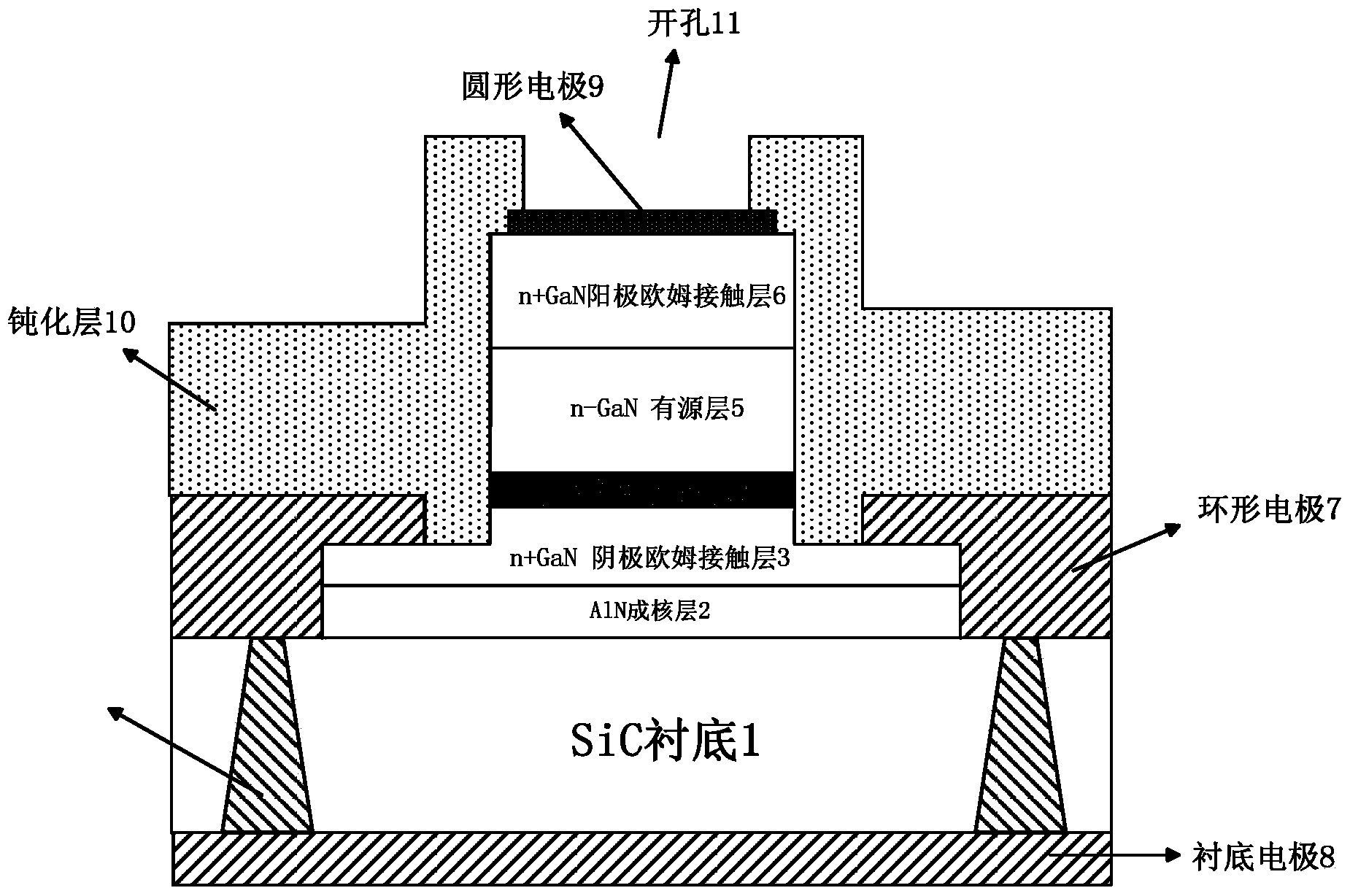
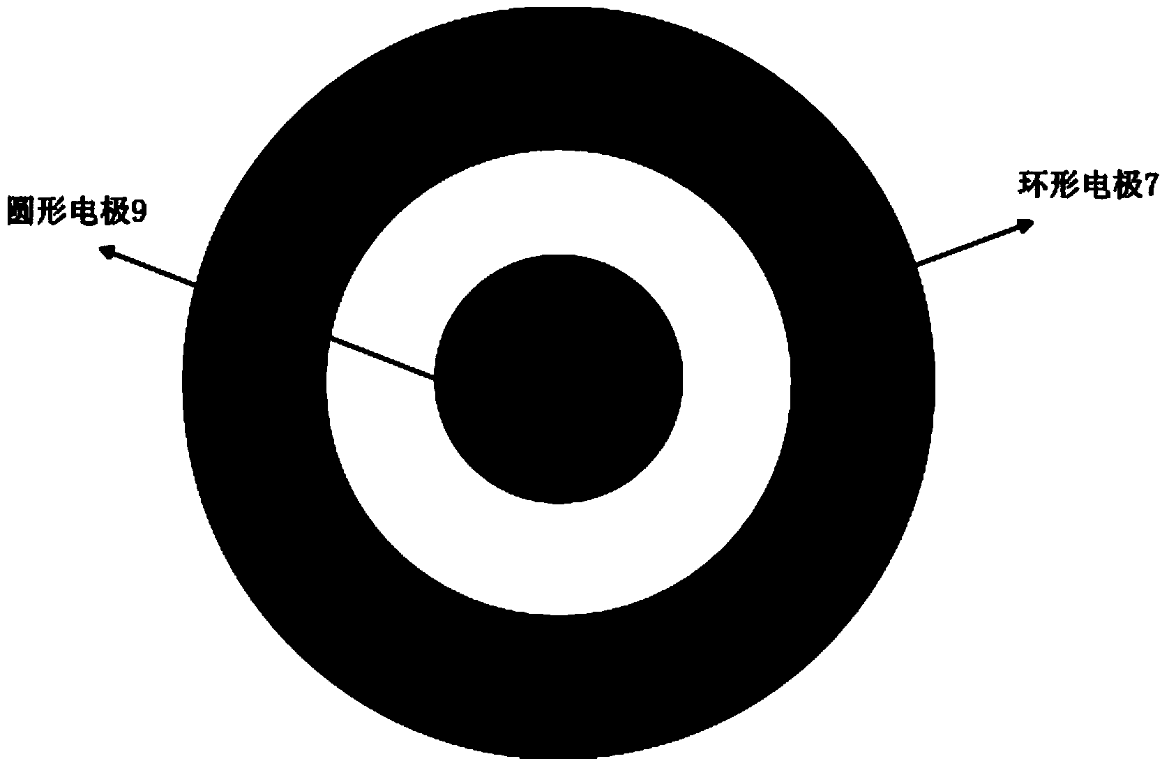
GaN Gunn diode based on AlGaN/GaN superlattice electron emission layer and manufacturing method
A technology of electron emission layer and Gunn diode, which is applied in the direction of circuits, electrical components, bulk negative resistance effect devices, etc., can solve the problems that are not considered, affect the electrical characteristics of terahertz devices, and cannot significantly reduce the dislocation concentration. Effect of small lattice mismatch and reduction of dislocation concentration
- Summary
- Abstract
- Description
- Claims
- Application Information
AI Technical Summary
Problems solved by technology
Method used
Image
Examples
Embodiment 1
[0057] Embodiment 1: Fabricate a GaN Gunn diode on a 4H-SiC semi-insulating substrate.
[0058] Step 1, select a 4H-SiC semi-insulating substrate with a diameter of 2 inches, and thin the back surface until the thickness of the substrate is 150 μm.
[0059] Step 2, put the 4H-SiC semi-insulating substrate into the MOCVD reaction chamber, set the growth temperature to 600°C, feed trimethylaluminum and nitrogen into the reaction chamber at the same time, and grow under the condition of maintaining the pressure at 40 Torr AlN nucleation layer with a thickness of 30 nm.
[0060] Step 3: Raise the substrate on which the AlN nucleation layer has been grown to 1000°C, simultaneously inject trimethylgallium, nitrogen and n-type dopant source-silane into the reaction chamber, and keep the pressure at 40Torr , with a growth thickness of 100 nm and a doping concentration of 1.0×10 18 cm -3 the n + GaN cathode ohmic contact layer.
[0061] Step 4, put the sample obtained in the above...
Embodiment 2
[0072] Embodiment 2: Fabricate a GaN Gunn diode on a 6H-SiC semi-insulating substrate.
[0073] Step 1, thinning the substrate:
[0074] A 6H-SiC semi-insulating substrate with a diameter of 2 inches is selected, and the back surface is thinned until the thickness of the substrate is 150 μm.
[0075] Step 2, epitaxially growing the AlN nucleation layer:
[0076] Using MOCVD, under the conditions of maintaining a pressure of 40Torr and a temperature of 650°C, trimethylaluminum and nitrogen are fed simultaneously to grow an AlN nucleation layer with a thickness of 40nm on a 6H-SiC semi-insulating substrate.
[0077] Step three, epitaxial growth n + GaN cathode ohmic contact layer:
[0078]Using MOCVD, raise the temperature to 1060°C, keep the pressure at 40Torr, and feed trimethylgallium, nitrogen and n-type dopant source—silane at the same time, the epitaxial growth thickness is 150nm, and the doping concentration is 1.5 ×10 18 cm -3 the n + GaN cathode ohmic contact lay...
Embodiment 3
[0107] Embodiment 3: Fabricate a GaN Gunn diode on a 6H-SiC conductive substrate.
[0108] Step A, thinning the substrate:
[0109] A 6H-SiC conductive substrate with a diameter of 2 inches is selected, and the back surface is thinned until the thickness of the substrate is 150 μm.
[0110] Step B, making AlN nucleation layer and n + GaN cathode ohmic contact layer:
[0111] In the MOCVD reaction chamber, under the conditions of keeping the pressure at 60 Torr and the temperature at 650°C, feed trimethylaluminum and nitrogen at the same time, and grow an AlN nucleation layer with a thickness of 90nm on the 6H-SiC conductive substrate; continue Using MOCVD process, raise the temperature to 1100℃, keep the pressure at 60Torr, and then feed trimethylgallium, nitrogen and n-type dopant source - silane at the same time, and epitaxially grow n + GaN cathode ohmic contact layer, the thickness of the ohmic contact layer is 400nm, and the doping concentration is 2×10 18 cm -3 .
...
PUM
| Property | Measurement | Unit |
|---|---|---|
| Thickness | aaaaa | aaaaa |
| Thickness | aaaaa | aaaaa |
| Thickness | aaaaa | aaaaa |
Abstract
Description
Claims
Application Information
 - R&D
- Intellectual Property
- Life Sciences
- Materials
- Tech Scout
- Unparalleled Data Quality
- Higher Quality Content
- 60% Fewer Hallucinations
Browse by: Latest US Patents, China's latest patents, Technical Efficacy Thesaurus, Application Domain, Technology Topic, Popular Technical Reports.
© 2025 PatSnap. All rights reserved.Legal|Privacy policy|Modern Slavery Act Transparency Statement|Sitemap|About US| Contact US: help@patsnap.com


