Micro-bubble generator and manufacturing method thereof
A technology of micro-bubble generator and double-layer graphene, which is applied in the field of micro-electromechanical systems, can solve the problems of easy corrosion and high power consumption, and achieve the effects of not easy electrolysis or corrosion, prolonging life, and flexible design
- Summary
- Abstract
- Description
- Claims
- Application Information
AI Technical Summary
Problems solved by technology
Method used
Image
Examples
preparation example Construction
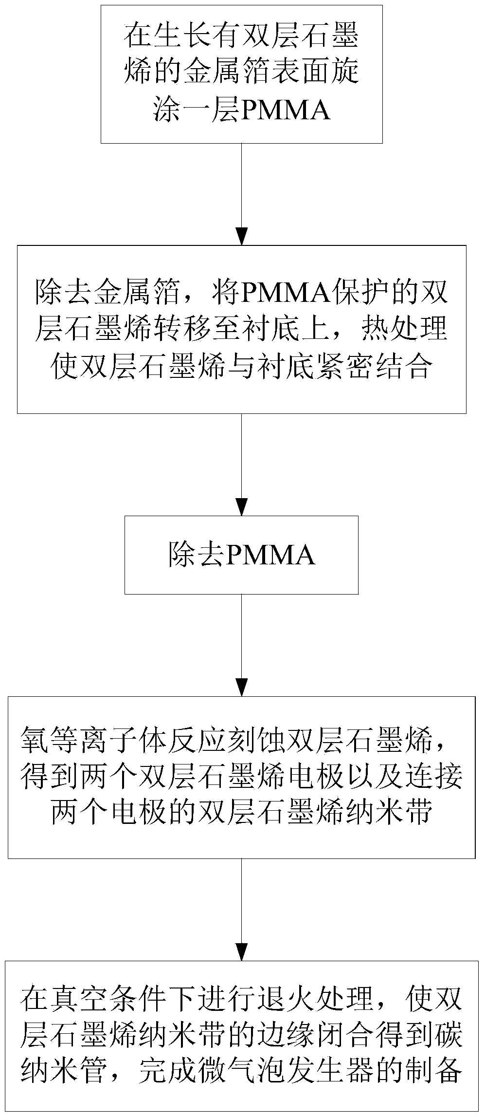
[0019] Such as figure 1 and figure 2 As shown, the preparation method of the microbubble generator of the embodiment of the present invention comprises the following steps:
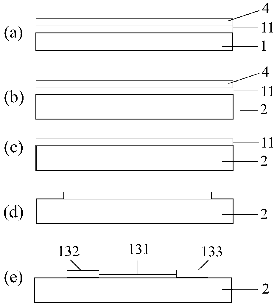
[0020] (1) Spin-coat a layer of PMMA4 on the surface of the metal foil 1 growing double-layer graphene 11, such as figure 2 (a) shown.
[0021] (2) Corrode the metal foil 1 with ferric chloride or ammonium persulfate solution to obtain the double-layer graphene 11 protected by PMMA4, wash it with deionized water, transfer it to the substrate 2 cleaned according to the standard CMOS process, and heat-treat Make bilayer graphene 11 and substrate 2 tightly combined, as figure 2 (b) shown.
[0022] (3) PMMA4 is removed by soaking in acetone, and the bilayer graphene 11 transferred to the substrate 2 is obtained, such as figure 2 (c) shown.
[0023] (4) Oxygen plasma reaction etches the double-layer graphene 11 to obtain two double-layer graphene electrodes and a double-layer graphene nanoribbon conn...
Embodiment 1
[0030] The preparation method of microbubble generator comprises the steps:
[0031] (1) Spin-coat a layer of PMMA with a thickness of about 200 nm on the surface of copper foil with double-layer graphene.
[0032] (2) Use 0.5mol / L ammonium persulfate solution to corrode the metal foil to obtain PMMA-protected double-layer graphene, wash it with deionized water for 3 times, transfer it to the substrate cleaned by the standard CMOS process, blow After drying, bake at 150°C for 10 minutes to make the double-layer graphene tightly bond with the substrate.
[0033] (3) PMMA was removed by immersion in acetone for 1 h, and bilayer graphene transferred to the substrate was obtained.
[0034] (4) Cover the double-layer graphene with silicon oxide nanowires as a mask, and react the oxygen plasma to etch the double-layer graphene to obtain two double-layer graphene electrodes and a double-layer graphene nanoribbon connecting the two electrodes, The distance between the two electrodes...
Embodiment 2
[0037] The preparation method of microbubble generator comprises the steps:
[0038] (1) Spin-coat a layer of PMMA with a thickness of about 200 nm on the surface of copper foil with double-layer graphene.
[0039] (2) Etch the metal foil with 0.5mol / L ammonium persulfate solution to obtain PMMA-protected double-layer graphene, wash it with deionized water for 4 times, transfer it to the substrate cleaned by the standard CMOS process, blow After drying, bake at 150°C for 10 minutes to make the double-layer graphene tightly bond with the substrate.
[0040] (3) PMMA was removed by immersion in acetone for 1 h, and bilayer graphene transferred to the substrate was obtained.
[0041] (4) Cover the double-layer graphene with silicon oxide nanowires as a mask, and react the oxygen plasma to etch the double-layer graphene to obtain two double-layer graphene electrodes and a double-layer graphene nanoribbon connecting the two electrodes, The distance between the two electrodes is 8...
PUM
| Property | Measurement | Unit |
|---|---|---|
| width | aaaaa | aaaaa |
Abstract
Description
Claims
Application Information
 - R&D
- Intellectual Property
- Life Sciences
- Materials
- Tech Scout
- Unparalleled Data Quality
- Higher Quality Content
- 60% Fewer Hallucinations
Browse by: Latest US Patents, China's latest patents, Technical Efficacy Thesaurus, Application Domain, Technology Topic, Popular Technical Reports.
© 2025 PatSnap. All rights reserved.Legal|Privacy policy|Modern Slavery Act Transparency Statement|Sitemap|About US| Contact US: help@patsnap.com


