Method for manufacturing uncooled infrared focal plane array pixel with silicon-germanium film

An uncooled infrared, focal plane array technology, applied in the field of infrared imaging device manufacturing, to achieve the effects of increased resistance, high TCR value, and good performance

Active Publication Date: 2014-04-16
NANJING UNIV OF SCI & TECH
View PDF7 Cites 6 Cited by
  • Summary
  • Abstract
  • Description
  • Claims
  • Application Information

AI Technical Summary

Problems solved by technology

[0004] The purpose of the present invention is to provide a method for manufacturing an uncooled infrared focal plane array pixel using a quantum well type silicon germanium thin film material, so as to solve the engineering application problem of quantum well materials with excellent performance in the field of uncooled infrared focal plane manufacturing

Method used


Image

  • Method for manufacturing uncooled infrared focal plane array pixel with silicon-germanium film
  • Method for manufacturing uncooled infrared focal plane array pixel with silicon-germanium film
  • Method for manufacturing uncooled infrared focal plane array pixel with silicon-germanium film

Examples


Embodiment Construction

[0037] The present invention will be described in further detail below in conjunction with the accompanying drawings.

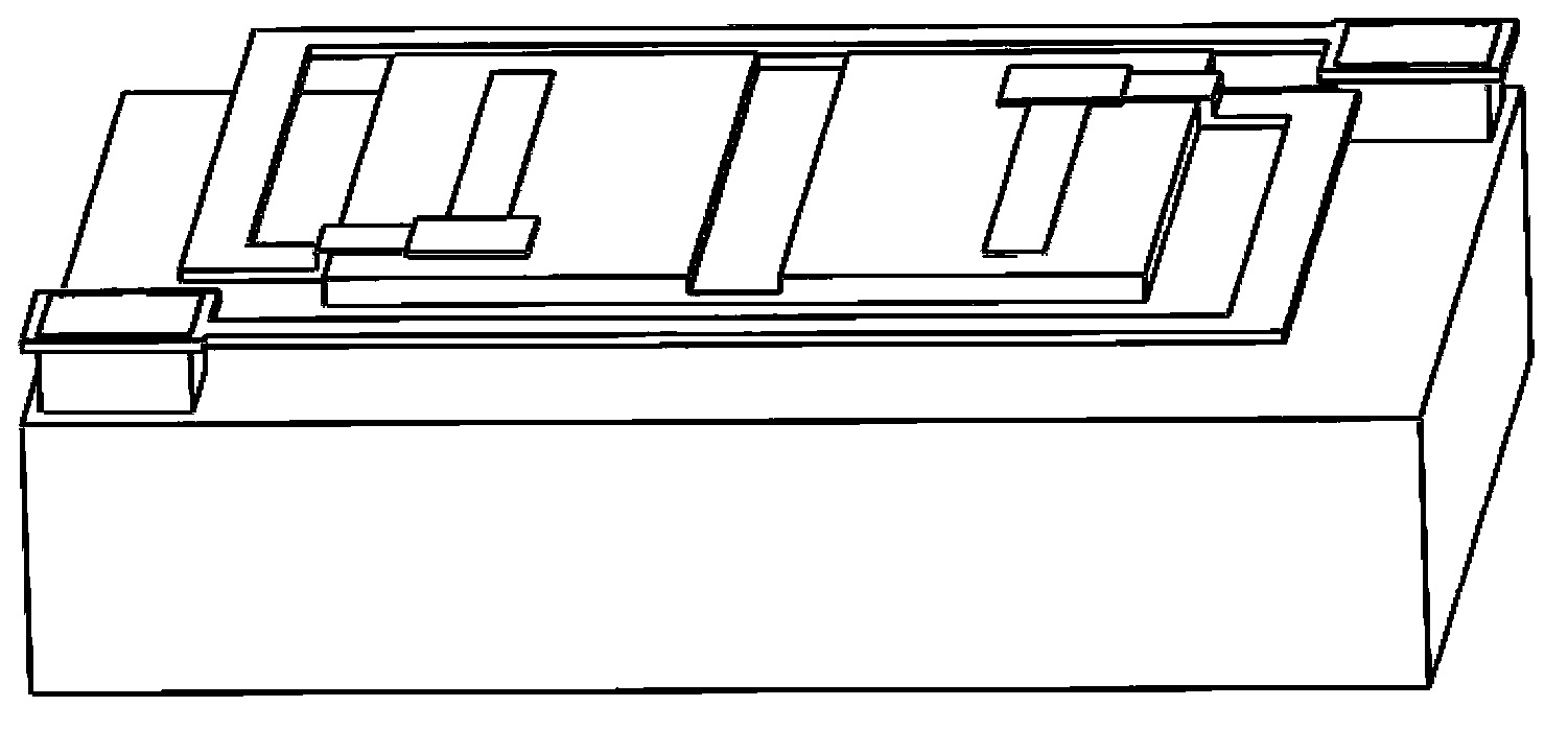
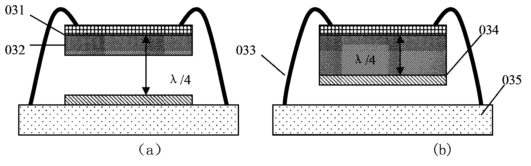
[0038] combine Figure 4 , the present invention is an uncooled infrared focal plane manufacturing pixel method using a silicon germanium film. Now, taking a 40×40 μm pixel as an example, the array manufacturing process is briefly described:

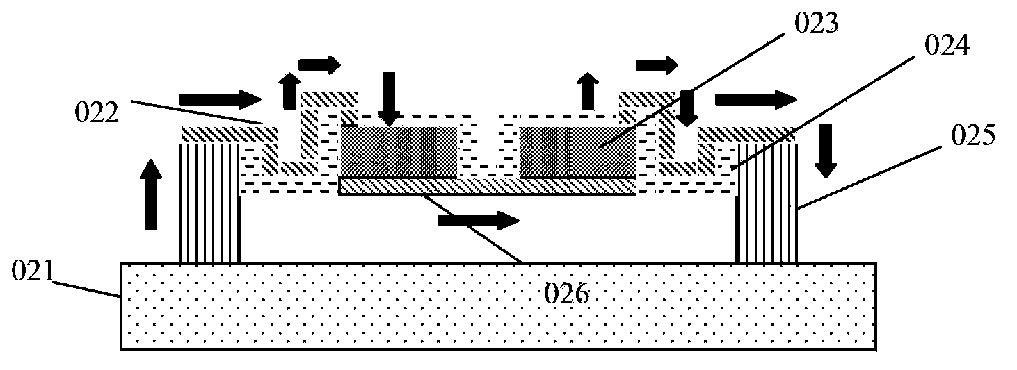
[0039]Step 1: Use SOI (Silicon-On-Insulator, silicon on insulating substrate) wafer as the carrier of quantum well type silicon germanium film 043, and apply bonding glue on the surface of the wafer to form a bond with a thickness of 1 μm-3 μm glue layer 048, and bond the SOI wafer and CMOS readout circuit 047 together by thermocompression adhesive bonding, and then use an ICP etching machine to etch away the SOI wafer silicon substrate 041, and then use BOE solution (Buffered Oxide Etch, composed of hydrofluoric acid and ammonium fluoride solution in a certain volume ratio, the usual ratio is 6:1) or BHF solution (dil...


PUM


Abstract

The invention discloses a method for manufacturing an uncooled infrared focal plane array pixel with a silicon-germanium film. The method includes the steps of transferring the silicon-germanium film to a CMOS wafer from an SOI wafer, etching the silicon-germanium film to form a channel, forming a metal top electrode with a lift-off method, etching the silicon-germanium film to form a sensitive block, depositing a silicon nitride supporting film with a PECVD method, carrying out electroplating to grow metal electrode columns, sputtering TiW to form a circuit, sputtering an infrared absorption layer, etching a silicon nitride layer, a TiW layer and the like, forming an L-shaped cantilever beam and the like. According to the method, silicon-germanium / silicon quantum well materials are successfully applied to the field of micrometering bolometers, and the range of sensitive materials capable of being used for making an uncooled infrared focal plane is expanded; it is considered that the silicon-germanium / silicon quantum well materials are three-dimensional electric conducting materials, a U-shaped loop is formed in the mode of etching the channel, and the resistance of the sensitive area is improved; the silicon nitrogen film is introduced, a lambda / 4 resonance infrared absorption cavity is formed in the sensitive area, the size of the infrared absorption cavity is accurately controlled, and the infrared absorption rate is effectively improved.

Description

technical field [0001] The invention belongs to the field of microelectronic processing technology applied to the manufacture of infrared imaging devices, and relates to a method for manufacturing an uncooled infrared focal plane array pixel using a TCR (temperature coefficient of resistance) silicon-germanium quantum well material as a sensitive material. Background technique [0002] Infrared imaging technology has a wide range of applications and demands in military and civilian fields. Infrared imaging reflects the information of thermal radiation on the surface of an object and its internal heat dissipation. It is an extension of people's vision beyond the visible light band and a new means of observing and perceiving the objective world. With the breakthrough of infrared sensitive material technology and the rapid development and maturity of MEMS manufacturing technology, miniature bolometers have been widely used in military and civilian fields, such as thermal imagin...

Claims


Application Information

Patent Timeline
IPC IPC(8): H01L31/18H01L27/146
CPCH01L31/035254H01L31/035281H01L31/1804Y02P70/50
Inventor 何勇苏岩方中董涛王开鹰杨朝初
Owner NANJING UNIV OF SCI & TECH
Why Eureka
Try Eureka