Method for manufacturing Cu2ZnSn(S, Se)4 solar battery absorbing layer through oxide thin film in vulcanizing and selenizing mode
A technology of oxide thin films and solar cells, which is applied in the field of solar photovoltaic materials, can solve problems such as human body and environmental hazards, and achieve low cost, wide applicability, and good crystallinity
- Summary
- Abstract
- Description
- Claims
- Application Information
AI Technical Summary
Problems solved by technology
Method used
Image
Examples
preparation example Construction
[0027] The present invention provides a low-cost, high-quality Cu 2 ZnSn(S,Se) 4 The preparation method of the thin film is simple in operation, convenient in controlling the stoichiometric ratio of elements, the precursor material used is low in cost and non-toxic, and the prepared thin film has uniform thickness and good crystallinity.
[0028] The method of the present invention is that metal precursor metal salt is dissolved in alcoholic solution, then obtains uniform oxide film with spin-coating method, then carries out sulfide-selenization to obtain high-quality Cu 2 ZnSn(S,Se) 4 Film absorber.
[0029] Specifically, as an example, the preparation method of the present invention may include the following steps.
[0030] First, the metal reactant precursors copper salt, zinc salt, and tin salt are represented by Cu 2 ZnSn(S,Se) 4 The stoichiometric ratio of Cu, Zn, and Sn in the solution is dissolved in the first solvent (such as ethanol), and then stirred until the ...
Embodiment 1
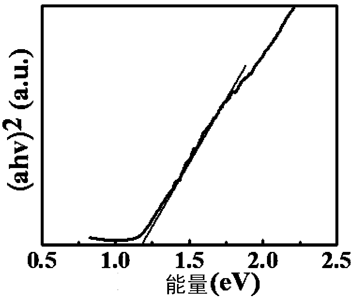
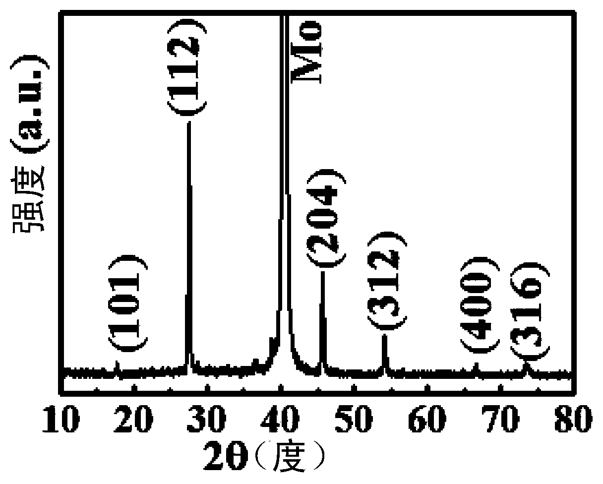
[0047] Add the reactant precursor 100ml ethanol, 1mmol copper acetate, 0.5mmol zinc acetate, 0.5mmol tin tetrachloride, 10ml ethylene glycol and 10ml propylene glycol into the reagent bottle in turn, stir at room temperature for 60 minutes until the solution is completely clear, and then add Spin coating on molybdenum substrate at a speed of 1000 rpm to form a film. After heating on a heating plate at 350°C, a uniform oxide film was obtained. Sulfurization and selenization annealing were carried out for 30 minutes under certain temperature conditions to obtain a thin film of the absorbing layer. The scanning electron microscope image of the absorbing film is shown in figure 1 It can be seen from the figure that the film distribution of the absorbing layer is uniform. figure 2 The optical bandgap diagram calculated from the absorption data of the absorbing layer thin film is shown. It can be seen from the figure that the forbidden bandwidth is about 1.2eV. image 3 Show the ...
Embodiment 2
[0049] Add reactant precursor 20ml methanol, 0.2mmol copper acetate, 0.1mmol zinc acetate, 0.1mmol tin dichloride, 2ml ethylene glycol and 2ml propylene glycol into the reagent bottle in turn, stir at room temperature for 10 minutes until the solution is completely clear, then Spin-coat a film on a molybdenum substrate at a speed of 500 rpm, and obtain a uniform oxide film after heating on a heating plate at 200 ° C. Repeat the above spin-coating steps for 5 times and then in a nitrogen atmosphere of 10,000 Pa, 450 Sulfurization and selenization annealing are carried out under the temperature condition of ℃ for 10 minutes to obtain the absorption layer thin film.
PUM
 Abstract
Description
Claims
Application Information
 - R&D
- Intellectual Property
- Life Sciences
- Materials
- Tech Scout
- Unparalleled Data Quality
- Higher Quality Content
- 60% Fewer Hallucinations
Browse by: Latest US Patents, China's latest patents, Technical Efficacy Thesaurus, Application Domain, Technology Topic, Popular Technical Reports.
© 2025 PatSnap. All rights reserved.Legal|Privacy policy|Modern Slavery Act Transparency Statement|Sitemap|About US| Contact US: help@patsnap.com


