A junction-modulated tunneling field-effect transistor and its manufacturing method

A tunneling field effect and transistor technology, which is used in the manufacture of diodes, semiconductor devices, semiconductor/solid-state devices, etc., can solve the problems of sub-threshold slope degradation of TFETs, limiting the application of TFET devices, and insufficient electric field at the tunnel junction, etc. Effects of reduced subthreshold slope, narrow tunneling barrier width, and suppression of bipolar conduction effects

Active Publication Date: 2016-02-17
PEKING UNIV
View PDF6 Cites 0 Cited by
  • Summary
  • Abstract
  • Description
  • Claims
  • Application Information

AI Technical Summary

Problems solved by technology

TFET has many excellent characteristics such as low leakage current, low subthreshold slope, low operating voltage, and low power consumption. However, due to the limitation of source junction tunneling probability and tunneling area, TFET faces the problem of small on-state current, far It is not as good as traditional MOSFET devices, which greatly limits the application of TFET devices
In addition, TFET devices with a steep subthreshold slope are also difficult to realize experimentally, because it is difficult to achieve a steep doping concentration gradient at the source junction so that the electric field at the tunnel junction is not large enough when the device is turned on. This causes the subthreshold slope of the TFET to degrade from the theoretical value

Method used


Image

  • A junction-modulated tunneling field-effect transistor and its manufacturing method
  • A junction-modulated tunneling field-effect transistor and its manufacturing method
  • A junction-modulated tunneling field-effect transistor and its manufacturing method

Examples


Embodiment Construction

[0038] The present invention will be further described below by example. It should be noted that the purpose of the disclosed embodiments is to help further understand the present invention, but those skilled in the art can understand that various replacements and modifications are possible without departing from the spirit and scope of the present invention and the appended claims of. Therefore, the present invention should not be limited to the content disclosed in the embodiments, and the protection scope of the present invention is subject to the scope defined in the claims.

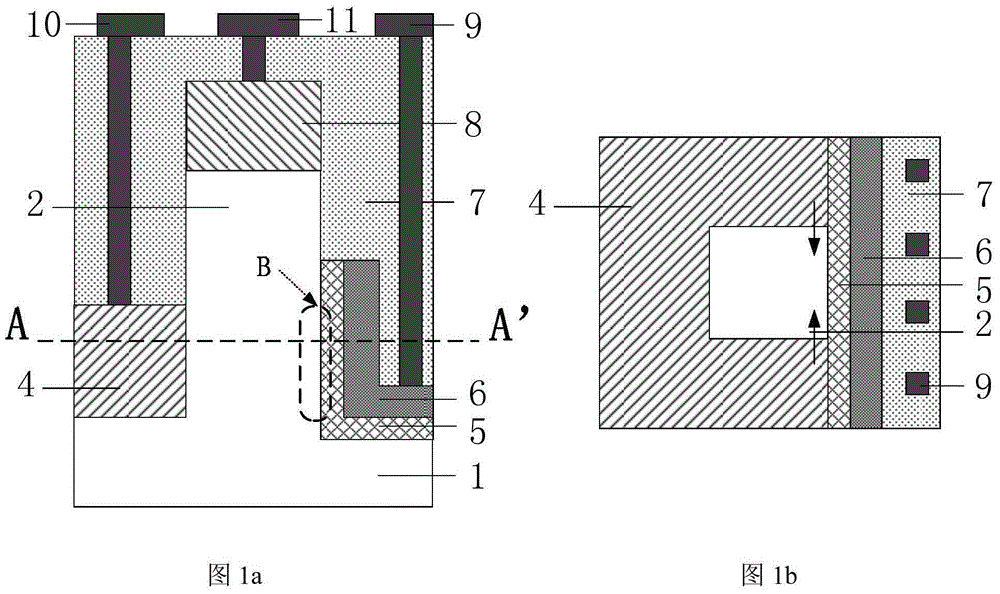
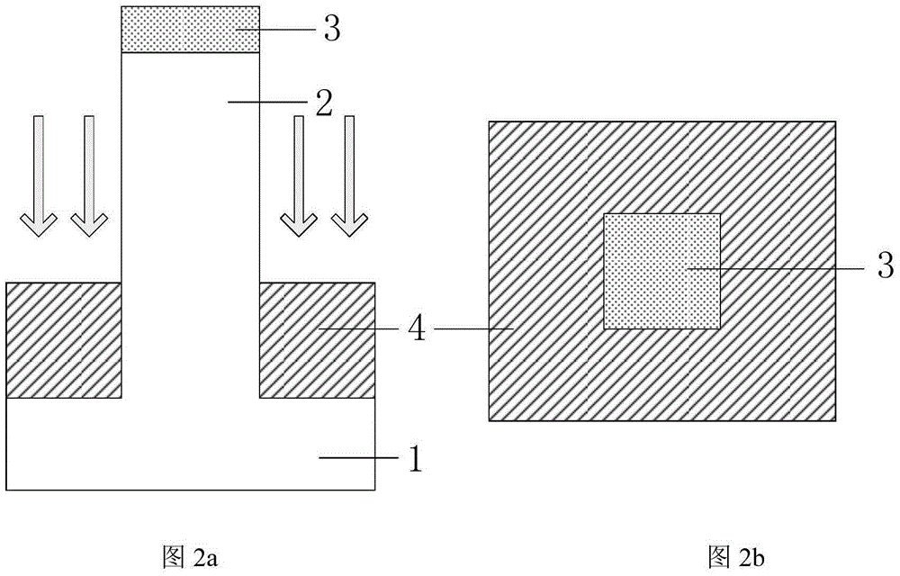
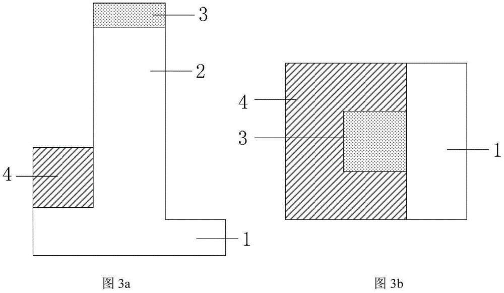
[0039] A specific example of the preparation method of the present invention includes Fig. 2 to Figure 7 Process steps shown:

[0040] 1. Deposit a hard mask layer 3 on a bulk silicon wafer silicon substrate 1 with a crystal orientation of (100), and the hard mask layer is Si 3 N 4 , the thickness is 300nm, and the doping concentration of the substrate is lightly doped; then photolithography is ...


PUM


Abstract

The invention discloses a junction modulation type tunneling field effect transistor and a preparation method thereof, belonging to the field of field effect transistor logic devices and circuits in CMOS ultra large integrated circuits (ULSI). The tunneling field effect transistor utilizes the PN junction provided by the highly doped source region surrounded on three sides of the vertical channel region to effectively deplete the channel region, so that the channel energy band on the lower surface of the gate is increased, and when the device undergoes band tunneling, it can obtain The steeper energy band and narrower tunneling barrier width than traditional TFETs equivalently realize the effect of steep tunneling junction doping concentration gradient, thereby greatly improving the subthreshold characteristics of traditional TFETs and improving the conductance of the device at the same time. Pass current. Under the condition of being compatible with the existing CMOS technology, the present invention effectively suppresses the bipolar conduction effect of the device on the one hand, and at the same time suppresses the parasitic tunneling current at the corner of the source junction in a small size, and can equivalently realize steep The effect of straight source-junction doping concentration.

Description

technical field [0001] The invention belongs to the field of field effect transistor logic devices and circuits in CMOS ultra large integrated circuits (ULSI), and in particular relates to a junction modulation type tunneling field effect transistor and a preparation method thereof. Background technique [0002] Driven by Moore's Law, the feature size of traditional MOSFETs has been shrinking, and now it has entered the nanometer scale. As a result, the negative effects of short-channel effects on devices have become more serious. The leakage-induced barrier reduction, band-band tunneling and other effects make the off-state leakage current of the device continuously increase. At the same time, the sub-threshold slope of the traditional MOSFET is limited by the thermoelectric potential and cannot be reduced synchronously with the shrinking of the device size, thus increasing device power consumption. The power consumption problem has become the most severe problem limiting ...

Claims


Application Information

Patent Timeline
Patent Type & Authority Patents(China)
IPC IPC(8): H01L21/336H01L29/78H01L29/06
CPCH01L29/0603H01L29/66356H01L29/7391H01L29/0657H01L29/0676H01L29/1033H01L21/266H01L21/3065H01L21/3085H01L21/324H01L29/0847H01L29/36H01L29/66666H01L29/66977H01L29/7827
Inventor 黄如黄芊芊吴春蕾王佳鑫詹瞻王阳元
Owner PEKING UNIV
Why Eureka
Try Eureka