Eureka AIR delivers breakthrough ideas for toughest innovation challenges, trusted by R&D personnel around the world.

Wafer-processing tape and method for manufacturing semiconductor device using same

A technology of wafer processing and manufacturing methods, which is applied in semiconductor/solid-state device manufacturing, semiconductor devices, film/sheet-like adhesives, etc. It can solve the problems that the adhesive layer cannot be cut and the chip cannot be peeled off, and the peeling force can be achieved. The effect of adequate, good pickup performance

Active Publication Date: 2013-12-18
FURUKAWA ELECTRIC CO LTD
View PDF9 Cites 21 Cited by
  • Summary
  • Abstract
  • Description
  • Claims
  • Application Information

AI Technical Summary

Problems solved by technology

This is because when the interface between the adhesive layer and the adhesive layer deviates, sufficient pulling force cannot be transmitted to the adhesive layer at that point, and the adhesive layer cannot be cut.
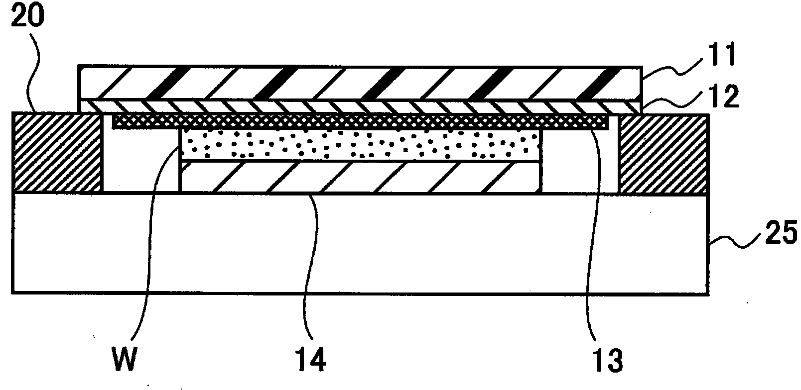
[0011] However, in general, when using a tape for wafer processing that is designed so that the interface between the adhesive layer and the adhesive layer does not shift, there is a problem that the chip that is divided in the pick-up process cannot be peeled off.

Method used


Image

  • Wafer-processing tape and method for manufacturing semiconductor device using same
  • Wafer-processing tape and method for manufacturing semiconductor device using same
  • Wafer-processing tape and method for manufacturing semiconductor device using same

Examples


Embodiment 1

[0188] With respect to 100 parts by mass of the acrylic copolymer (a-1), 5 parts by mass of CORONATE L (manufactured by Japan Polyurethane Co., Ltd.) was added as polyisocyanate, and 3 parts by mass of IRGACURE-184 (manufactured by Japan Ciba-Geigy Co., Ltd.) was added as photopolymerization initiator, the mixture was dissolved in ethyl acetate and stirred to prepare an adhesive composition.

[0189] Next, the pressure-sensitive adhesive composition was coated on a release liner made of a polyethylene terephthalate film subjected to mold release so that the thickness after drying was 10 μm, and dried at 110° C. for 3 minutes. After that, it was bonded to the base film to produce a PSA sheet in which the PSA layer was formed on the base film.

[0190] Next, the adhesive composition (d-1) was coated on a release liner made of a release-treated polyethylene terephthalate film so that the thickness after drying was 20 μm. Drying was carried out for 5 minutes to prepare an adhesiv...

Embodiment 2

[0193] Except having used the acrylic-type copolymer (a-2), it carried out similarly to Example 1, and prepared the adhesive composition. Using this adhesive composition, by the method similar to Example 1, the tape for wafer processing was produced.

Embodiment 3

[0195] Except having used the acrylic-type copolymer (a-3), it carried out similarly to Example 1, and prepared the adhesive composition. Using this adhesive composition, by the method similar to Example 1, the tape for wafer processing was produced.


PUM

PropertyMeasurementUnit
peel strengthaaaaaaaaaa
densityaaaaaaaaaa
Vicat softening pointaaaaaaaaaa

Abstract

The purpose of the present invention is to provide a wafer-processing tape that does not result in displacement at the interface between the adhesive layer and the sticky agent layer due to expansion, that has uniform expansion properties suitable for a step for dividing the adhesive layer, and that has excellent pickup performance. In the present invention, the wafer-processing tape is characterized by comprising: a substrate film; a sticky agent layer formed on the substrate film; and an adhesive layer formed on the sticky agent layer; the shear force of the sticky agent layer and the adhesive layer at 25 DEG C being no less than 0.2 N / mm2, and the peeling force between the sticky agent layer and the adhesive layer at a peeling angle of 180 DEG and a peeling speed of 300 mm / min in a standard state compliant with JIS-Z0237 after being irradiated by an energy beam of 200 mJ / cm2 being no greater than 0.3 N / 25 mm.

Description

technical field [0001] The present invention relates to an expandable wafer processing tape or the like used when an adhesive layer is cut along a chip by expansion in a manufacturing process of a semiconductor device. Background technique [0002] In the manufacturing process of semiconductor devices such as ICs, the following processes are carried out: back grinding process, which grinds the back of the wafer to make the wafer thinner after the circuit pattern is formed; After processing the tape, the wafer is cut into chip units; the expansion process is to expand (expand) the tape for wafer processing; the pick-up process is to pick up the cut chip; the die bonding (mount) process, further Bond the picked-up chip to a lead frame or package substrate (or, in a stacked package, laminate and bond chips to each other). [0003] In the above-mentioned back grinding process, a surface protection tape is used to protect the circuit pattern formation surface (wafer surface) of ...

Claims


Application Information

Patent Timeline
Patent Type & Authority Applications(China)
IPC IPC(8): H01L21/301C09J4/00C09J7/02C09J133/00C09J161/28C09J163/00C09J175/04C09J201/02H01L21/304H01L21/52
CPCC08G18/6229C08G18/6705C08G18/8029C08G18/8116C08L75/00C09J4/00C09J7/385C09J133/14C09J161/28C09J175/14C09J2203/326H01L21/6836H01L24/27H01L24/83H01L2221/68327H01L2221/6834H01L2221/68381H01L2224/2919H01L2224/83191H01L2924/12042H01L2924/181H01L2924/00C08F220/1812C08F220/20C08F220/06C08F220/1808C09J7/20
Inventor 佐野透石黑邦彦三原尚明井之前千佳子矢吹朗建部一贵
Owner FURUKAWA ELECTRIC CO LTD
Why Eureka
Eureka Blog
Learn More