Multi-ceramic layer led packaging structure

A technology of LED packaging and ceramic layer, which is applied in the electronic field, can solve problems such as crack failure, ceramic layer cracks, and difficult performance requirements, and achieve the effects of improving wettability, solving heat dissipation problems, and improving reliability

Active Publication Date: 2015-11-18
上海晶擎能源科技有限公司
View PDF5 Cites 0 Cited by
  • Summary
  • Abstract
  • Description
  • Claims
  • Application Information

AI Technical Summary

Problems solved by technology

With the development of optical and / or electronic devices, their performance requirements are becoming more and more stringent, such as the need to further improve the integration of integrated circuits, the need to improve the luminous efficiency of LEDs, etc., so that the ceramic intermediate layer The performance requirements are also getting higher and higher. For example, as a ceramic intermediate layer, it not only needs to have high thermal conductivity and electrical insulation rate, but also needs to have high voltage breakdown strength, and also needs to have fluorescence characteristics; these properties require a single ceramic function. Layers are often difficult to achieve, and studies have also shown that it is difficult to meet all requirements through composite ceramic coatings, and composite ceramic coatings often have large differences in thermal expansion coefficients of various components, and the internal heat produced by repeated cycles of different temperatures Stress can cause cracks in the ceramic layer and even lead to fracture failure

Method used


Image

  • Multi-ceramic layer led packaging structure

Examples


Embodiment 1

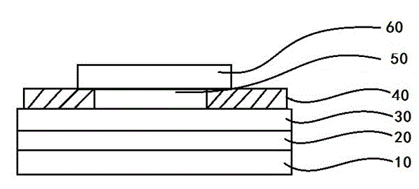
[0021] The multi-ceramic layer LED packaging structure described herein includes a metal base 10, and a pressure-resistant ceramic layer 20 and a high thermal conductivity ceramic layer 30 are sequentially formed on the metal base 10, and a high thermal conductivity ceramic layer 30 is formed on the high thermal conductivity ceramic layer 30. A metal circuit layer 40 and a fluorescent ceramic layer 50 ; and an LED chip 60 is arranged on the metal circuit layer 40 and the fluorescent ceramic layer 50 . The metal matrix can be metal matrixes such as Al, Cu, Ag and Ni or their alloy matrix; the metal circuit layer is formed by dry etching through a deposited conductive metal layer, and the conductive metal is usually preferably Cu, Ag, Al or their alloy materials. In the multi-ceramic layer LED packaging structure, the multi-ceramic layers are all formed by a known sintering method, and the fluorescent ceramic layer is a Ce-doped YAG layer, and the Ce-doped YAG layer is cerium-do...

Embodiment 2

[0023] The multi-ceramic layer LED packaging structure described herein includes a metal base 10, and a pressure-resistant ceramic layer 20 and a high thermal conductivity ceramic layer 30 are sequentially formed on the metal base 10, and a high thermal conductivity ceramic layer 30 is formed on the high thermal conductivity ceramic layer 30. A metal circuit layer 40 and a fluorescent ceramic layer 50 ; and an LED chip 60 is arranged on the metal circuit layer 40 and the fluorescent ceramic layer 50 . The metal matrix can be metal matrixes such as Al, Cu, Ag and Ni or their alloy matrix; the metal circuit layer is formed by dry etching through a deposited conductive metal layer, and the conductive metal is usually preferably Cu, Ag, Al or their alloy materials. In the multi-ceramic layer LED packaging structure, the multi-ceramic layers are all formed by a known sintering method, and the fluorescent ceramic layer is a Eu-doped SiN layer, and the Eu-doped SiN layer is formed by...


PUM


Abstract

The invention relates to a multi-ceramic-layer LED packaging structure which comprises a metal substrate, wherein a voltage-withstanding ceramic layer and a high heat-conducting ceramic layer are sequentially formed on the metal substrate; a metal circuit layer and a fluorescent ceramic layer are formed on the high heat-conducting ceramic layer; and an LED chip is arranged on the metal circuit layer and the fluorescent ceramic layer. The printed circuit board has multiple functional ceramic layers, and fulfills aims of thermal conductivity, resistance to high-voltage breakdown and improvement of luminous efficiency.

Description

technical field [0001] The invention belongs to the field of electronic technology, and more specifically, the invention relates to a multi-ceramic layer LED packaging structure for optical devices. Background technique [0002] Devices used in optics and / or electronics, such as integrated circuits or laser diodes, require the use of thermally conductive materials for heat transfer. For this purpose, a metallic base body is used, for example a copper base body, and an electrical isolation is often required between the optical and / or electronic components and the metal base body. And some ceramic materials have higher heat transfer efficiency and are electrically insulating. For this purpose, highly thermally conductive ceramic materials are frequently used as intermediate materials for providing electrical isolation while still maintaining thermal conductivity between the optical and / or electronic components and the metal base body. In order to provide efficient heat trans...

Claims


Application Information

Patent Timeline
Patent Type & Authority Patents(China)
IPC IPC(8): H01L33/48H01L33/50H01L33/64
Inventor 高鞠
Owner 上海晶擎能源科技有限公司
Why Eureka
Try Eureka