BCD semiconductor device and manufacturing method thereof

A technology of semiconductors and devices, which is applied in the field of semiconductor power devices, can solve problems such as limitations and rise in on-resistance, achieve high withstand voltage, reduce specific on-resistance, and reduce manufacturing costs

Inactive Publication Date: 2013-10-02
SHENZHEN LAND HOPE MICRO ELECTRONICS
View PDF5 Cites 15 Cited by
  • Summary
  • Abstract
  • Description
  • Claims
  • Application Information

AI Technical Summary

Problems solved by technology

However, due to the specific on-resistance (Specific on-resistance, R on,sp ) and device breakdown voltage (Breakdown Voltage, BV) exist R on,sp ∝BV 2.3~2.6 The relationship between the device makes the on-resistance rise sharply when the device is applied at high voltage, which limits the application of lateral high-voltage DMOS devices in high-voltage power integrated circuits, especially in circuits that require low conduction loss and small chip area

Method used


Image

  • BCD semiconductor device and manufacturing method thereof

Examples


Embodiment Construction

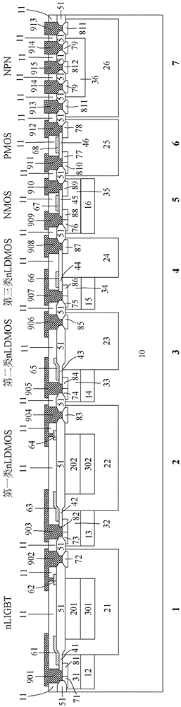
[0031] The invention provides a novel BCD semiconductor device, such as figure 1 Shown:

[0032] The high-voltage nLIGBT device 1 is directly built in the p-type substrate 10, the n-type heavily doped layer 201 is located under the field oxide layer 51 and surrounded by the n-type drift region well 21; the p-type drop field layer 301 is located on the n-type heavily doped Below the miscellaneous layer 201; p + The anode region 72 is under the anode metal 902 and surrounded by the n-type drift region well 21; n + Cathode region 81 and p + The well contact region 71 is located side by side under the cathode metal 901 and surrounded by the p-type body region 31; the polysilicon gate 61 is partly on the gate oxide layer 41 and partly on the field oxide layer 51; between the cathode metal 901, the anode metal 902 and the polysilicon gate 61 are isolated from each other by a pre-metal dielectric 11.

[0033] The first type of high-voltage nLDMOS device 2 is directly made in the ...


PUM


Abstract

The invention relates to a BCD semiconductor device and a manufacturing method thereof. The BCD semiconductor device comprises a high voltage nLIGBT device (1), a first type of high voltage nLDMOS device (2), a second type of nLDMOS device (3), a third type of nLDMOS device (4), a low voltage NMOS device (5), a low voltage PMOS device (6) and a low voltage NPN device (7), wherein n-type drift region wells (21, 22) of the high voltage nLIGBT device (1) and of the first type of high voltage nLDMOS device (2) are respectively introduced with n-type heavily-doped layers (201, 202), and p-type reduced-field layers (301, 302) are respectively arranged below the n-type heavily-doped layers (201, 202) and are surrounded by the n-type drift region wells (21, 22). A smaller conduction resistance is realized while chip areas are the same, or a smaller chip area is realized while conduction capabilities are the same. The BCD semiconductor device has advantages of simple manufacturing method and relatively less difficult technology.

Description

technical field [0001] The invention belongs to the technical field of semiconductor power devices, and relates to a BCD (Bipolar CMOS DMOS) device and a manufacturing method thereof. Background technique [0002] High-voltage power integrated circuits often use the high analog precision of Bipolar transistors, the high integration of CMOS, and the high power or voltage characteristics of DMOS (Double-diffused MOSFET) to integrate Bipolar analog circuits, CMOS logic circuits, CMOS analog circuits and DMOS high-voltage power devices. Monolithically integrated together (referred to as BCD device). Lateral high-voltage devices are widely used in high-voltage power integrated circuits because the drain, gate, and source are all on the chip surface, and are easy to integrate with low-voltage signal circuits through internal connections. However, due to the specific on-resistance (Specific on-resistance, R on,sp ) and device breakdown voltage (Breakdown Voltage, BV) exist R on,...

Claims


Application Information

Patent Timeline
Patent Type & Authority Applications(China)
IPC IPC(8): H01L27/06H01L29/06H01L29/10H01L21/8249
Inventor 乔明李燕妃许琬陈涛张波
Owner SHENZHEN LAND HOPE MICRO ELECTRONICS
Why Eureka
Try Eureka