Preparation method of CIGS (copper indium gallium selenide) thin-film solar cell absorbing layer
A technology of solar cells and copper indium gallium selenide, which is applied in the field of solar cells, can solve problems such as difficulties in the industrialization of copper indium gallium selenide thin-film solar cells, rough CIGS thin film surfaces, environmental pollution, etc., and achieve low cost, high repeatability, and reduced pollution effect
- Summary
- Abstract
- Description
- Claims
- Application Information
AI Technical Summary
Problems solved by technology
Method used
Image
Examples
Embodiment 1
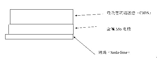
[0036]The film samples were obtained by DC magnetron sputtering and radio frequency magnetron sputtering on the JGP-450 magnetron sputtering deposition system. The sputtering targets were high-purity (99.99% ) metal molybdenum (Mo) target and high-purity (99.99%) copper indium gallium selenide (CuIn 0.7 Ga 0.3 Se 2 ) quaternary alloy target, using a square Soda-lime glass with a side length of 2.5 cm and a thickness of 1 mm as the substrate. Before putting the soda-lime glass into the chamber, it was cleaned with acetone ultrasonically for 20 min, and then with alcohol ultrasonically. 5 minutes and blow dry. The background vacuum of the experiment is 4.0×10 -4 Pa, before depositing the Mo film, the substrate was bias cleaned for 15 min, the air pressure during cleaning was 2.0 Pa, and the bias voltage was -400 V. During the deposition of the film, the substrate is continuously rotated to improve the uniformity of the film. At room temperature, a Mo back electrode with a...
Embodiment 2
[0039] The film samples were obtained by DC magnetron sputtering and radio frequency magnetron sputtering on the JGP-450 magnetron sputtering deposition system. The sputtering targets were high-purity (99.99% ) metal molybdenum (Mo) target and high-purity (99.99%) copper indium gallium selenide (CuIn 0.7 Ga 0.3 Se 2 ) quaternary alloy target, using a square Soda-lime glass with a side length of 2.5 cm and a thickness of 1 mm as the substrate. Before putting the soda-lime glass into the chamber, it was cleaned with acetone ultrasonically for 20 min, and then with alcohol ultrasonically. 5 minutes and blow dry. The background vacuum of the experiment is 4.0×10 -4 Pa, before depositing the Mo film, the substrate was bias cleaned for 15 min, the air pressure during cleaning was 2.0 Pa, and the bias voltage was -400 V. During the deposition of the film, the substrate is continuously rotated to improve the uniformity of the film. At room temperature, a Mo back electrode with ...
Embodiment 3
[0041] The film samples were obtained by DC magnetron sputtering and radio frequency magnetron sputtering on the JGP-450 magnetron sputtering deposition system. The sputtering targets were high-purity (99.99% ) metal molybdenum (Mo) target and high-purity (99.99%) copper indium gallium selenide (CuIn 0.7 Ga 0.3 Se 2 ) quaternary alloy target, using a square Soda-lime glass with a side length of 2.5 cm and a thickness of 1 mm as the substrate. Before putting the soda-lime glass into the chamber, it was cleaned with acetone ultrasonically for 20 min, and then with alcohol ultrasonically. 5 minutes and blow dry. The background vacuum of the experiment is 4.0×10 -4 Pa, before depositing the Mo film, the substrate was bias cleaned for 15 min, the air pressure during cleaning was 2.0 Pa, and the bias voltage was -400 V. During the deposition of the film, the substrate is continuously rotated to improve the uniformity of the film. At room temperature, a Mo back electrode with ...
PUM
 Abstract
Description
Claims
Application Information
 - R&D Engineer
- R&D Manager
- IP Professional
- Industry Leading Data Capabilities
- Powerful AI technology
- Patent DNA Extraction
Browse by: Latest US Patents, China's latest patents, Technical Efficacy Thesaurus, Application Domain, Technology Topic, Popular Technical Reports.
© 2024 PatSnap. All rights reserved.Legal|Privacy policy|Modern Slavery Act Transparency Statement|Sitemap|About US| Contact US: help@patsnap.com


