
Preparation method of tapered zinc oxide/nickel oxide heterojunction diode

A technology of zinc oxide and heterojunction, which is applied in the direction of electrical components, circuits, semiconductor devices, etc., can solve the problems of difficulty in preparing ZnO homojunction diodes and the lack of stable preparation methods, and achieve high luminous efficiency

Active Publication Date: 2016-08-03
南通东湖国际商务服务有限公司
View PDF5 Cites 5 Cited by
  • Summary
  • Abstract
  • Description
  • Claims
  • Application Information

AI Technical Summary

Problems solved by technology

[0002] Zinc oxide (ZnO) is a direct wide bandgap compound semiconductor material, its room temperature bandgap is 3.37ev, and the exciton binding energy is 60mev, so ZnO is an ideal material for semiconductor lasers at room temperature and higher temperatures; intrinsic ZnO is a transparent n-type semiconductor, but so far, there is no stable p-type ZnO preparation method, so it is very difficult to prepare ZnO homojunction diodes; and intrinsic nickel oxide (NiO) is a p-type Semiconductor material with a direct bandgap of 3.7eV, p-type NiO and n-type ZnO can form heterojunction diodes; due to the wide bandgap characteristics of ZnO and NiO, they have good thermal and chemical stability, and there is no environment during the preparation process Pollution, so that the heterojunction diode composed of NiO and ZnO has considerable advantages

Method used


Image

  • Preparation method of tapered zinc oxide/nickel oxide heterojunction diode
  • Preparation method of tapered zinc oxide/nickel oxide heterojunction diode
  • Preparation method of tapered zinc oxide/nickel oxide heterojunction diode

Examples


example 1

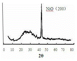
[0020] 1. Form a 200nm thick NiO layer on the nickel sheet by thermal oxidation

[0021] Put the nickel sheet with a pointed surface structure into a heating furnace and heat it in the air at a heating temperature of 450 o C, heating time 45mim.

[0022] 2. Using ALD technology to prepare 80nm thick ZnO

[0023] Deposition conditions: reaction temperature 200°C, Zn(CH 2 CH 3 ) 2 (DEZ) for 1s, nitrogen purge for 1.5s, water flow for 500ms, nitrogen purge for 1s, repeat the above process 800 times.

[0024] 3. Preparation of ITO transparent upper electrode by sputtering method

[0025] ITO target is used, argon is used as sputtering gas; firstly, the background vacuum of the chamber is evacuated to 1′10 -4 Pa, argon gas is introduced, the working pressure of argon gas is 1.5Pa, the sputtering power is 60w, the sputtering time is 20min, and the electrode thickness is 100nm.

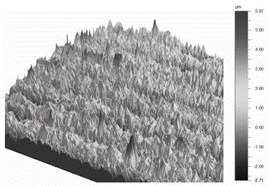
[0026] 4. Using femtosecond laser processing technology to form a pointed cone columnar structure ...


PUM

PropertyMeasurementUnit
heightaaaaaaaaaa
thicknessaaaaaaaaaa

Abstract

The invention relates to the preparation technology of heterojunction ultraviolet laser diodes, in particular to a method for preparing pointed-cone-shaped p-NiO (nickel oxide) / n-ZnO (zinc oxide) heterojunctions by combining the film coating technology and the femtosecond laser technology. According to the method, firstly, heat oxidation is utilized to form a NiO layer on a nickel sheet, then, an atomic layer deposition method is utilized for preparing a ZnO layer, next, an ITO (indium tin oxide) transparent upper electrode is formed outside the n-type ZnO layer by a sputtering method, finally, a pointed-cone-shaped array is formed on the nickel sheet covered with an NiO / ZnO / ITO layer by the femtosecond laser processing technology, pointed-cone-shaped p-NiO / n-ZnO heterojunctions are formed, voltage is applied to the ITO and the bottom of the nickel sheet, and the electroluminescence can be realized.

Description

technical field [0001] The invention relates to a preparation technology of a heterojunction ultraviolet laser diode, in particular to the preparation of a tapered p-NiO / n-ZnO heterojunction by combining coating technology and femtosecond laser technology. Background technique [0002] Zinc oxide (ZnO) is a direct wide bandgap compound semiconductor material, its room temperature bandgap is 3.37ev, and the exciton binding energy is 60mev, so ZnO is an ideal material for semiconductor lasers at room temperature and higher temperatures; intrinsic ZnO is a transparent n-type semiconductor, but so far, there is no stable p-type ZnO preparation method, so it is very difficult to prepare ZnO homojunction diodes; and intrinsic nickel oxide (NiO) is a p-type Semiconductor material with a direct bandgap of 3.7eV, p-type NiO and n-type ZnO can form heterojunction diodes; due to the wide bandgap characteristics of ZnO and NiO, they have good thermal and chemical stability, and there is...

Claims


Application Information

Patent Timeline
Patent Type & Authority Patents(China)
IPC IPC(8): H01L33/00H01L33/24H01L33/38
Inventor 袁宁一房香丁建宁陈梦蛟邱建华
Owner 南通东湖国际商务服务有限公司
Learn More